

Why Is Large Size HDI PCB Crucial for High-Density and High-Speed Applications?
2025-07-14
What makes a large size HDI PCB different from standard PCBs?
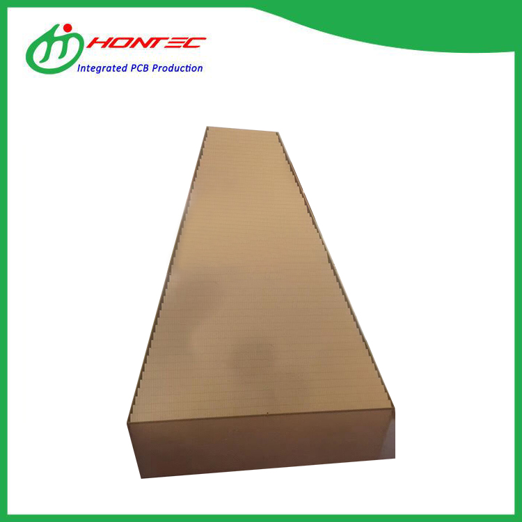
Having worked in the PCB manufacturing field for over 20 years, I’ve seen how the demand for large size HDI PCB has grown significantly. Unlike conventional boards, these PCBs support high-density interconnects on an expanded surface area, which is ideal for advanced communication systems, servers, and aerospace electronics.
Why is large size HDI PCB the ideal solution for complex circuitry?
When your design involves multiple ICs, high-speed signal transmission, and fine-pitch components, a large size HDI PCB becomes essential. It allows for more layers, finer lines, and tighter spacing, while minimizing signal interference. I’ve used HONTEC’s HDI solutions in high-frequency radar modules and was impressed by their precision and reliability.
What challenges does large size HDI PCB solve in industrial applications?
Traditional PCBs can’t always accommodate both the complexity and scale of modern systems. That’s where the large size HDI PCB comes in—it enables component placement without compromising signal integrity. With HONTEC, I’ve been able to eliminate bottlenecks in signal routing, which helped reduce design time and board rework.
Why is HONTEC a reliable choice for large size HDI PCB manufacturing?
I’ve worked with several PCB suppliers, and HONTEC consistently delivers when it comes to dimensional accuracy, microvia quality, and multilayer alignment. Their manufacturing of large size HDI PCBs is supported by advanced laser drilling, AOI inspection, and high-frequency material compatibility. Plus, their engineering team offers responsive DFM support.
Is a large size HDI PCB worth the investment for your next project?
Absolutely. Though slightly higher in cost than standard boards, the performance gain and space efficiency of large size HDI PCB far outweigh the expense—especially when you source from HONTEC, where quality and yield rates are unmatched.
Ready to take your complex PCB designs to the next level?
I highly recommend partnering with HONTEC for your large size HDI PCB requirements. Their engineering precision and customer service make them a standout in the global PCB market.
Our products are highly reliable. If you have any cooperation or bulk purchase needs, please contact us. We offer 24-hour online quality service.