

Why Is DIP PCB Assembly Still the Backbone of Reliable Electronic Manufacturing Today?
2025-10-24
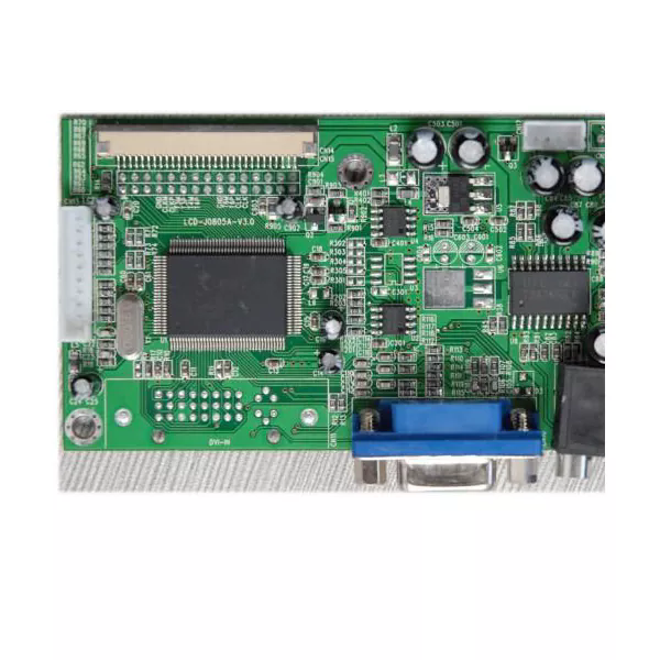
DIP PCB Assembly, short for Dual In-line Package Printed Circuit Board Assembly, remains one of the most dependable and cost-effective methods for producing electronic devices with stable performance. Unlike surface-mount technology (SMT), DIP PCB Assembly involves inserting electronic components—such as resistors, capacitors, transistors, and integrated circuits—through pre-drilled holes on the PCB. These components are then soldered on the opposite side to ensure mechanical strength and reliable electrical connectivity.
The reason DIP assembly continues to hold strong relevance in a rapidly advancing electronics industry is its proven reliability, thermal stability, and ease of maintenance. It is the preferred choice for products requiring long-term durability under demanding environmental or mechanical stress, such as in automotive electronics, industrial control systems, power modules, and military-grade equipment.
Why Choose DIP PCB Assembly Over Surface-Mount Technology (SMT)?
While SMT has dominated high-speed automated assembly lines, DIP PCB Assembly continues to thrive due to its unique combination of durability, precision, and cost-efficiency for certain product categories.
Here are some key reasons why DIP assembly remains relevant and widely adopted:
-
Mechanical Stability:
Components inserted through holes and soldered on both sides provide superior resistance to vibration and mechanical stress. This is crucial for applications exposed to motion or shocks. -
Ease of Prototyping and Testing:
Engineers favor DIP assemblies for prototypes and small production runs because components can be manually inserted, adjusted, and replaced during testing phases. -
High Power Handling:
Through-hole connections allow for higher current flow compared to surface-mounted joints, making DIP ideal for power electronics and high-voltage applications. -
Thermal Management:
The deeper solder joints in DIP assemblies facilitate better heat dissipation, enhancing component lifespan and operational stability. -
Serviceability and Maintenance:
Unlike SMT boards, DIP assemblies can be easily repaired or reworked, minimizing downtime and replacement costs.
Typical Industries Using DIP PCB Assembly
-
Industrial automation and control systems
-
Automotive electronics and power supplies
-
Medical devices with low-volume, high-reliability demands
-
Aerospace communication and navigation systems
-
Audio amplifiers, power converters, and analog modules
What Are the Technical Specifications and Parameters Defining DIP PCB Assembly?
To ensure consistent performance and manufacturing precision, DIP PCB Assembly adheres to rigorous technical standards. Below is a detailed overview of key parameters and features that define the process quality:
| Parameter | Description |
|---|---|
| Component Type | Through-hole components (ICs, resistors, diodes, capacitors, connectors) |
| Hole Size Tolerance | ±0.05 mm for accurate component alignment |
| PCB Thickness | 1.0 mm – 3.2 mm depending on design and layer count |
| Soldering Method | Wave soldering or selective soldering |
| Copper Thickness | 1 oz to 3 oz, depending on current requirements |
| Layer Count | Single, double, or multilayer PCB supported |
| Solder Mask Color Options | Green, Blue, Black, Red, White (customized available) |
| Assembly Accuracy | ±0.1 mm component placement tolerance |
| Testing Methods | ICT (In-Circuit Testing), AOI (Automated Optical Inspection), and functional testing |
| Lead-Free Compliance | RoHS-compliant soldering materials available |
| Operating Temperature Range | -40°C to +125°C, suitable for industrial and automotive environments |
Each assembly stage—from component insertion to wave soldering and inspection—is performed under controlled conditions to ensure optimal electrical performance, longevity, and safety compliance.
How Does the DIP PCB Assembly Process Work?
The DIP PCB Assembly process integrates manual craftsmanship with automated precision to create robust, reliable electronic circuits. Each step is essential for ensuring consistent solder quality and long-term stability.
1. PCB Preparation and Inspection
The process begins with the selection and visual inspection of the PCB base material. Engineers verify hole alignment, copper thickness, and surface finish to ensure readiness for assembly. Any contamination or residue is removed before component insertion.
2. Component Insertion
Electronic components are inserted manually or by semi-automated machines into the pre-drilled holes. Each component must match its designated orientation and polarity to ensure proper functionality. Skilled operators handle sensitive components such as ICs and capacitors to prevent electrostatic damage.
3. Wave Soldering
Once all components are placed, the board is passed through a wave soldering machine. The solder wave melts solder alloy and bonds component leads to copper pads on the PCB underside. This ensures strong mechanical connections and excellent electrical continuity.
4. Cleaning and Inspection
Post-soldering cleaning removes any flux residues to prevent corrosion or electrical leakage. Automated Optical Inspection (AOI) and X-ray analysis may be used to detect solder bridges, cold joints, or misaligned components.
5. Functional Testing
Functional testing validates the electrical behavior of the assembled PCB. Engineers conduct in-circuit testing (ICT) and signal performance analysis to ensure compliance with design requirements. Only boards that pass all quality checks proceed to the packaging stage.
6. Packaging and Delivery
After final inspection, DIP-assembled PCBs are packaged using ESD-safe materials and labeled according to traceability standards for shipment to global clients.
What Are the Future Trends in DIP PCB Assembly Technology?
Although the electronics industry continues to evolve toward miniaturization, DIP PCB Assembly remains vital for certain high-reliability applications. Modern innovations are transforming traditional DIP production into a hybrid model that combines manual precision with automation and data analytics.
1. Integration of AI-Assisted Quality Control
Machine learning algorithms are increasingly used to detect soldering defects and placement errors. These systems reduce human inspection time and improve yield rates.
2. Lead-Free and Environmentally Sustainable Manufacturing
Global regulatory frameworks, such as RoHS and REACH, are pushing manufacturers to adopt eco-friendly soldering materials and cleaner production technologies.
3. Hybrid Assembly Solutions
Some manufacturers are integrating both DIP and SMT components on the same PCB, creating hybrid assemblies that leverage the strengths of both methods—mechanical robustness and miniaturization.
4. Enhanced Automation for High-Mix, Low-Volume Production
Modern DIP assembly lines now feature semi-automated insertion systems that increase efficiency for small and medium production runs while maintaining flexibility for custom projects.
5. Advanced Thermal and Electrical Design Integration
Thermal simulation tools and precision copper balancing techniques are improving the thermal distribution and electrical efficiency of DIP assemblies, particularly for power electronics.
6. Global Supply Chain and Component Traceability
With growing demands for quality assurance, manufacturers are adopting digital traceability systems that record every stage of component handling—from sourcing to testing and delivery.
These advancements ensure that DIP PCB Assembly continues to evolve, meeting the reliability and sustainability needs of modern industries.
Common Questions About DIP PCB Assembly
Q1: What are the main differences between DIP and SMT assemblies?
A1: DIP (Dual In-line Package) uses through-hole technology where components are inserted into drilled holes and soldered on the opposite side, providing higher mechanical stability. SMT (Surface-Mount Technology) involves mounting components directly on the PCB surface, suitable for high-density circuits. DIP is ideal for durable, high-power applications, while SMT fits compact and high-speed electronics.
Q2: Can DIP PCB Assembly be used in high-frequency applications?
A2: While DIP is traditionally used in analog and power circuits, it can support moderate-frequency operations depending on design parameters such as trace width, grounding techniques, and component layout. For extremely high-frequency applications (GHz range), SMT typically performs better due to reduced lead inductance.
How Hitech Enhances Reliability and Customization in DIP PCB Assembly
Hitech specializes in precision-engineered DIP PCB Assembly solutions, combining decades of manufacturing experience with advanced inspection and testing technologies. Each assembly undergoes comprehensive quality control to ensure compliance with international standards such as IPC-A-610, ISO 9001, and RoHS.
Hitech’s production capabilities include custom DIP assembly, mixed-technology boards, and lead-free wave soldering, designed to meet the specific needs of industries ranging from industrial control to automotive electronics. With a focus on flexibility, scalability, and reliability, Hitech offers end-to-end support—from PCB layout review and component sourcing to functional testing and packaging.
For businesses seeking durable, high-performance, and cost-effective PCB assembly solutions, DIP technology remains an essential choice—and Hitech continues to lead the way in delivering trusted quality across every project.
Contact us to learn more about how Hitech’s DIP PCB Assembly solutions can optimize your product’s performance, reliability, and manufacturing efficiency.