

Why Is BGA PCB Assembly Revolutionizing the Future of Electronic Manufacturing?
2025-10-16
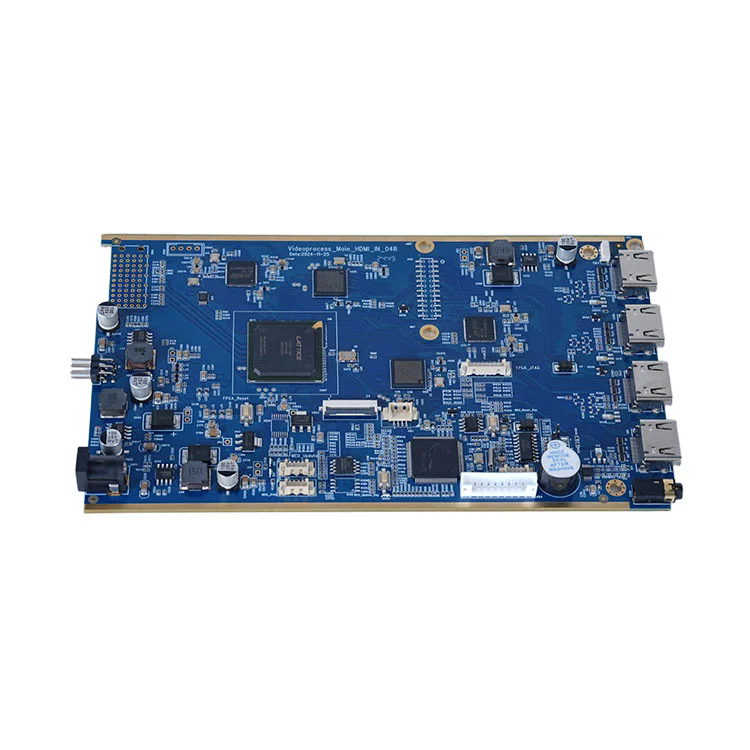
Ball Grid Array (BGA) PCB Assembly represents a significant evolution in printed circuit board technology. It is a type of surface-mount packaging used to permanently mount devices such as microprocessors onto printed circuit boards. Instead of using traditional leads or pins, BGA relies on tiny solder balls arranged in a grid pattern on the underside of the component. During the reflow soldering process, these balls melt and form reliable electrical and mechanical connections between the component and the PCB.
The growing demand for compact, high-performance devices — from smartphones and tablets to advanced automotive systems — has pushed manufacturers toward more efficient and powerful assembly methods. BGA PCB Assembly addresses the limitations of older packages like QFP (Quad Flat Package) or DIP (Dual In-line Package) by offering superior heat dissipation, reduced inductance, and increased interconnection density.
In the context of modern electronics manufacturing, BGA Assembly is not just a packaging method — it is the foundation of high-speed data processing, miniaturized circuit design, and efficient power management. The move toward BGA-based designs marks a pivotal shift toward smaller, smarter, and more efficient electronic devices.
How Does BGA PCB Assembly Work and What Makes It Technically Superior?
BGA PCB Assembly relies on a precise and systematic process that ensures accuracy, reliability, and long-term performance. Every step is critical, from design and fabrication to inspection and testing.
Process Overview:
| Step | Description | Technical Significance |
|---|---|---|
| 1. Solder Paste Application | A fine layer of solder paste is applied to the PCB pads using a stencil printer. | Ensures uniform solder distribution, critical for strong joints. |
| 2. Component Placement | The BGA component is aligned and placed on the board by automated pick-and-place machines. | Guarantees accurate positioning within microns of tolerance. |
| 3. Reflow Soldering | The PCB passes through a controlled temperature profile where solder balls melt and bond with the PCB pads. | Forms reliable electrical and mechanical connections. |
| 4. Inspection (X-Ray Testing) | X-ray imaging is used to detect voids, bridges, or open joints under the BGA. | Confirms hidden solder joint integrity and ensures reliability. |
| 5. Functional Testing | The assembled PCB is tested for performance and functionality. | Validates signal integrity and overall board performance. |
Key Technical Advantages:
-
Higher Interconnect Density:
BGA allows for hundreds or even thousands of solder connections in a compact footprint, optimizing circuit complexity without increasing board size. -
Improved Electrical Performance:
The short, uniform connections between the chip and board minimize signal distortion and enhance data transmission speeds. -
Superior Thermal Conductivity:
The design allows heat to dissipate more efficiently, preventing overheating and improving long-term reliability. -
Smaller Package Size:
By eliminating protruding leads, BGA assemblies support thinner and lighter device designs, ideal for modern electronics. -
Enhanced Reliability:
The use of solder balls distributes mechanical stress evenly across the component, reducing the risk of solder joint cracking.
BGA technology has thus become the preferred solution for high-performance products such as 5G communication systems, IoT devices, medical electronics, and automotive radar modules.
Why Is BGA PCB Assembly the Future of Advanced Electronics?
As the electronics industry evolves toward higher integration and miniaturization, BGA PCB Assembly continues to lead innovation. Its ability to deliver speed, reliability, and compactness aligns perfectly with the next generation of technology trends.
Emerging Trends and Market Direction:
-
Miniaturization of Devices
Wearables, smartphones, and medical implants are shrinking in size. BGA packaging allows more transistors in less space while maintaining stable electrical performance. -
Integration with AI and IoT
BGA-based boards power edge devices and AI accelerators, providing fast signal processing and low latency — key to real-time decision-making in IoT systems. -
Advanced Thermal Management
As processing speeds increase, so does heat generation. BGA’s ability to distribute thermal loads evenly makes it ideal for high-performance computing and automotive applications. -
5G and High-Frequency Applications
BGA PCBs ensure minimal electrical resistance and excellent high-frequency performance, crucial for 5G transceivers and baseband processors. -
Automotive and Aerospace Growth
BGA Assembly’s durability under vibration and temperature extremes makes it indispensable for automotive control units, radar modules, and avionics systems. -
Reliability Under Stress
With lead-free soldering and RoHS compliance, BGA PCBs meet global sustainability standards without compromising performance.
Future Outlook:
The next decade will see even more complex BGA-to-system integrations, such as PoP (Package-on-Package) and SiP (System-in-Package), where multiple BGAs stack vertically to create multi-functional modules. This 3D packaging evolution will drive further miniaturization and enhance computational density — an essential factor for AI-driven electronics and quantum computing modules.
Common Questions About BGA PCB Assembly
Q1: What are the main challenges in BGA PCB Assembly, and how are they solved?
A1: The most common challenges include solder joint defects, misalignment, and inspection difficulty. To mitigate these issues, manufacturers use X-ray imaging for non-destructive testing, precise thermal profiling during reflow soldering, and automated optical inspection systems. Additionally, modern assembly lines utilize computer vision for real-time monitoring, ensuring each joint meets IPC quality standards.
Q2: How does BGA PCB Assembly affect product lifespan?
A2: Properly executed BGA assembly significantly extends product life by improving electrical contact stability and thermal performance. The even distribution of solder joints minimizes mechanical stress, while enhanced heat dissipation prevents overheating. As a result, devices built with BGA assemblies exhibit longer operational lifespans and higher reliability in demanding environments.
How to Choose the Right BGA PCB Assembly Partner?
Selecting a manufacturing partner for BGA PCB Assembly requires careful consideration of both technical capability and production quality. The right assembler should demonstrate:
-
Experience with Fine-Pitch Components:
High-precision placement accuracy for micro BGAs (pitch below 0.5 mm). -
Advanced X-Ray and AOI Testing Capabilities:
To ensure zero-defect solder joint reliability. -
Certified Quality Systems:
Compliance with ISO, IPC-A-610, and RoHS environmental standards. -
Customized Prototyping and Volume Production:
Ability to scale from small-batch prototypes to full mass production. -
Thermal Management and Design Optimization Expertise:
Integration of thermal vias, copper pours, and controlled impedance design for optimal signal and heat performance.
Partnering with a company that invests in precision manufacturing equipment and R&D ensures consistent quality and innovation. The right partnership helps reduce time-to-market while maintaining cost efficiency and long-term reliability.
The Future of Electronics Built on BGA Technology
The ongoing evolution of microelectronics points to an era where BGA PCB Assembly will dominate advanced circuit integration. With increasing demands for compactness, performance, and energy efficiency, BGA is set to remain the backbone of semiconductor packaging for decades to come.
As AI, 5G, and autonomous systems accelerate global innovation, the need for robust, high-density interconnects becomes ever more critical. BGA technology provides the bridge between silicon performance and real-world functionality, turning complex circuitry into reliable, scalable solutions.
Conclusion – Building the Next Generation of Electronics with Fanway
From consumer electronics to automotive systems, BGA PCB Assembly defines the standard for high-performance, miniaturized, and reliable circuit integration. Its technical superiority, combined with evolving trends in microfabrication, positions it as the cornerstone of modern electronics manufacturing.
Fanway, with its deep expertise in advanced PCB assembly and precision manufacturing, delivers comprehensive BGA solutions tailored to diverse industrial needs. By combining quality assurance, state-of-the-art technology, and a commitment to innovation, Fanway ensures that every assembly meets the highest standards of durability and performance.
To discover how BGA PCB Assembly can elevate your electronic designs, contact us today and partner with Fanway to power the future of intelligent electronics.