

Why HDI PCBs Are the Future of Electronics Manufacturing
2025-08-14
The electronics industry is evolving rapidly, and High-Density Interconnect (HDI) PCBs are at the forefront of this transformation. As devices become smaller, faster, and more complex, traditional PCBs struggle to keep up. HDI PCBs, with their advanced design and manufacturing techniques, offer superior performance, reliability, and miniaturization. But why exactly are they becoming the go-to solution for modern electronics? Let’s dive deep into the reasons behind their growing dominance.
What Makes HDI PCBs Superior?
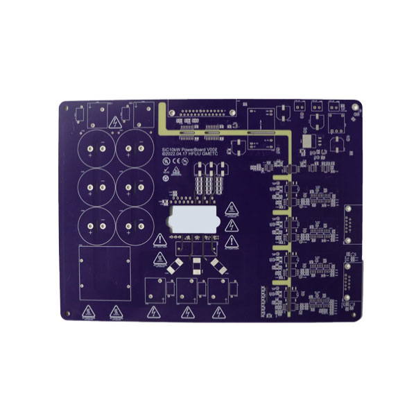
HDI PCBs are designed to accommodate more components in a smaller space, thanks to their high wiring density, microvias, and finer traces. These boards are essential for cutting-edge applications like smartphones, medical devices, and aerospace systems. Below are some key advantages:
Higher Circuit Density – More connections in a compact area.
Improved Signal Integrity – Reduced signal loss and interference.
Enhanced Thermal Performance – Better heat dissipation.
Lightweight & Miniaturized – Ideal for portable and space-constrained devices.
To better understand their technical superiority, here’s a breakdown of common HDI PCB specifications:
| Parameter | Standard Range | Advanced Options |
|---|---|---|
| Layer Count | 4-20 layers | Up to 30+ layers |
| Minimum Trace Width | 50µm (2 mil) | 25µm (1 mil) |
| Via Size (Microvia) | 100µm (4 mil) | 50µm (2 mil) |
| Material | FR4, High-Tg, Rogers | Flexible & Rigid-Flex |
| Surface Finish | ENIG, HASL, Immersion Tin | ENEPIG, Gold Plating |
How Are HDI PCBs Manufactured?
The production of HDI PCBs involves precision engineering and advanced techniques such as laser drilling, sequential lamination, and via-in-pad technology. Here’s a simplified overview:
-
Laser Drilling – Creates ultra-small microvias for high-density interconnects.
-
Sequential Lamination – Builds multiple layers with precise alignment.
-
Via Filling & Plating – Ensures reliable electrical connections.
-
Advanced Inspection – AOI and X-ray verification for defect-free boards.
This meticulous process ensures that HDI PCBs meet the strictest industry standards while delivering unmatched performance.
HDI PCB Common FAQs
Q: What industries benefit the most from HDI PCBs?
A: HDI PCBs are widely used in smartphones, wearables, medical implants, automotive radars, and military communications due to their compact size and high reliability.
Q: Are HDI PCBs more expensive than traditional PCBs?
A: Initially, yes—due to complex manufacturing. However, their long-term benefits, such as reduced size, weight, and improved performance, often justify the cost in high-end applications.
Why Choose Fanway for Your HDI PCB Needs?
At Fanway, we specialize in high-performance HDI PCBs tailored to your exact requirements. With state-of-the-art manufacturing facilities and a team of seasoned engineers, we ensure precision, durability, and cost-efficiency in every board we produce.
Whether you need prototypes or large-scale production, Fanway delivers on time, with rigorous quality checks at every stage.
Contact Us today to discuss your project needs and get a customized quote!