

Why Does My Flex PCB Prototype Fail After Bending
2026-06-16
When developing electronic devices, engineers often ask: Why does my Flex PCB Prototype fail after bending? At Hoshineo Lcd-Tech, we have analyzed hundreds of failed prototypes. The answer usually lies in material selection, bending radius, or copper layer design. Understanding these failure mechanisms is the first step toward a reliable Flex PCB Prototype.
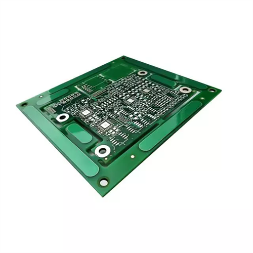
Top 5 Reasons for Bending-Related Failures
| Failure Mode | Typical Cause | Preventive Action |
|---|---|---|
| Copper Cracking | Bending radius < 5x material thickness | Increase bend radius to ≥ 10x thickness |
| Coverlay Delamination | Poor lamination pressure or temperature | Use controlled lamination cycles |
| Annular Ring Breakage | Copper fatigue near plated holes | Stagger vias away from bend area |
| Pad Lifting | Excessive mechanical stress on adhesives | Use dual-layer adhesive or adhesiveless material |
| Trace Necking | Uneven etching under bending zone | Add teardrops or rounded trace corners |
Core Engineering Principles for Reliable Bending
-
Minimum Bend Radius : Dynamic bending (repeated) needs radius ≥ 20x thickness; static bending (one-time) needs ≥ 10x thickness.
-
Neutral Bend Axis : Place neutral axis at the center of copper layer by balancing coverlay thickness on both sides.
-
Trace Routing : Route traces perpendicular to the bend line whenever possible. Never run wide traces parallel to a bending crease.
| Parameter | Dynamic Bending | Static Bending |
|---|---|---|
| Copper thickness (oz) | 0.5 max | 1.0 max |
| Base material (PI) | 25–50 µm | 25–75 µm |
| Bend cycles > 100k | Yes | Not required |
| Stiffener needed | No | Optional |
Flex PCB Prototype FAQ – Common Questions Answered
Q1: Can a Flex PCB Prototype fail after just one bending cycle even if the design passes all electrical tests?
A1: Yes. Electrical tests only verify continuity and isolation at zero stress. A single bend can introduce micro-cracks that close when the board is flat. These cracks grow over time or under temperature changes. The failure is mechanical first, electrical second. Always perform dynamic bend testing with at least 10,000 cycles using a bend tester, plus thermal shock (-40°C to 85°C, 10 cycles) before accepting a Flex PCB Prototype for production.
Q2: Why does my Flex PCB Prototype show intermittent signal loss after bending, even though the copper traces look intact under a microscope?
A2: Intermittent loss usually points to adhesive creep or dielectric compression in the bend area. When the board bends, the polyimide film and adhesive layers shift unevenly. This can change the characteristic impedance of high-speed traces (e.g., USB, MIPI) by ±15% or more. The copper may be fine, but the signal integrity fails. Solution: Use adhesiveless copper-clad laminates for bend zones, and simulate impedance change under bending in your CAD tool.
Q3: Is it possible to rework a failed Flex PCB Prototype by flattening and re-bending it carefully?
A3: Not recommended. Once copper grains have work-hardened from the first bend, the material loses ductility. Flattening creates new stress points. Re-bending almost always causes instant fatigue fracture. Instead, at Hoshineo Lcd-Tech, we suggest a design revision: increase bend radius by 30%, switch to rolled-annealed (RA) copper instead of ED copper, and add a backer stiffener 2 mm before the bend start line. No reliable repair process exists for a bended Flex PCB Prototype with internal cracks.
Final Checklist Before Ordering Your Next Flex PCB Prototype
-
Bend radius ≥ 10x (static) or 20x (dynamic) of total thickness
-
No vias or plated holes within 3 mm of bend area
-
Copper type: RA copper for dynamic bending
-
Coverlay extension: 1.5 mm past each bend end
-
Stress relief slits added on large copper areas
Get Your Flex PCB Prototype Right the First Time
Bending failures waste weeks of development time. At Hoshineo Lcd-Tech, we engineer Flex PCB Prototype solutions with failure analysis reports, material certificates, and dynamic bend testing. Contact us today for a free design review – send your Gerber files and bending requirements, and our engineers will fix weak points before manufacturing.