

Which Prototype PCB Assembly Process Delivers Reliable Results?
2026-11-11
Developing a new electronic product involves more than designing a circuit and sending files to a manufacturer. Before moving into mass production, engineers need to verify circuit performance, evaluate component compatibility, identify assembly issues, and confirm that the physical board meets the intended design requirements.Prototype PCB assembly plays a critical role in this process. It transforms a PCB design into a functional physical sample, allowing product developers to identify problems early, reduce engineering risks, and make informed decisions before committing to larger production volumes.
1. What Is Prototype PCB Assembly?
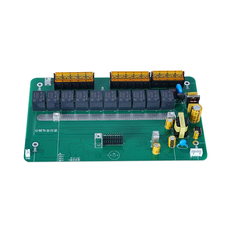
Prototype PCB assembly refers to the process of placing and soldering electronic components onto a printed circuit board in small quantities for product development and functional testing. Unlike high-volume manufacturing, prototype assembly focuses on flexibility, engineering verification, and identifying potential problems before production begins on a larger scale.
A prototype can range from a single experimental board to a small batch of assembled PCBs. The required quantity depends on the complexity of the project, the testing plan, and the development stage.
What Does a PCB Prototype Usually Include?
A typical assembled PCB prototype consists of several essential elements:
- Bare PCB: The fabricated circuit board with copper traces, solder pads, vias, and other designed structures.
- Electronic components: Integrated circuits, resistors, capacitors, connectors, sensors, and other devices.
- Solder connections: Electrical and mechanical connections that secure components to the board.
- Assembly configuration: Component placement, orientation, polarity, and mounting details.
- Inspection results: Visual or electrical verification to evaluate assembly quality.
Depending on the application, prototypes may use surface-mount technology (SMT), through-hole technology (THT), or a combination of both.
2. Why Is Prototype PCB Assembly Important?
Skipping prototype validation can expose a company to expensive engineering changes, production delays, and product reliability problems. A circuit that appears correct in design software may behave differently when assembled and operated under real conditions.
2.1 Identify Design Errors Before Mass Production
Even carefully reviewed PCB layouts can contain unexpected issues. Incorrect component footprints, reversed polarity, insufficient clearances, and routing problems may only become apparent during assembly or testing.
Building a prototype provides an opportunity to discover these problems while the design is still relatively easy to modify.
2.2 Verify Electrical and Functional Performance
A completed prototype allows engineers to test whether the board performs according to its intended specifications. Depending on the product, validation may include:
- Power supply stability and voltage regulation.
- Signal integrity and communication performance.
- Microcontroller and processor functionality.
- Sensor accuracy and response time.
- Thermal behavior under operating conditions.
- Compatibility with connected modules and external devices.
2.3 Reduce Development Costs and Production Risks
Finding a design problem after producing thousands of boards can result in significant rework, component replacement, and delivery delays. Prototype testing helps identify potential defects earlier, when corrective actions generally involve fewer units.
2.4 Improve Product Development Efficiency
Engineers can use prototype samples to compare different layouts, component selections, and circuit configurations. This creates a practical feedback loop between design, assembly, testing, and revision.
2.5 Confirm Manufacturing Feasibility
A design that works electrically may still be difficult to manufacture consistently. Prototype assembly helps evaluate component spacing, soldering accessibility, assembly tolerances, and the suitability of the chosen manufacturing process.
3. How Does the Prototype PCB Assembly Process Work?
A structured assembly workflow helps reduce misunderstandings, prevent component errors, and improve delivery predictability. Although specific procedures vary by manufacturer and board complexity, most prototype projects follow several key stages.
1 Design File Review
The process begins with reviewing the customer's PCB design files, bill of materials, and assembly requirements. Engineers check whether the supplied information is complete and whether the board can be manufactured and assembled as designed.
Potential concerns include missing component specifications, unclear polarity markings, footprint mismatches, and insufficient manufacturing information.
2 PCB Fabrication
After the design is confirmed, the bare PCB is manufactured according to the required specifications. Important parameters include:
- Board dimensions and thickness.
- Number of copper layers.
- Copper weight.
- Surface finish.
- Material selection.
- Minimum trace width and spacing.
These characteristics should match the electrical, mechanical, and environmental requirements of the application.
3 Component Sourcing and Verification
Components are sourced according to the approved bill of materials (BOM). Before assembly, manufacturers should verify part numbers, package types, quantities, and availability.
When an original component is unavailable, any proposed alternative should be reviewed and approved by the customer. Electrical characteristics, dimensions, operating temperature, and compatibility must be considered before substitution.
4 Solder Paste Printing
For SMT assembly, solder paste is applied to designated pads using a stencil. Accurate paste deposition is essential because insufficient or excessive solder paste can lead to defects such as poor joints, bridging, or component movement.
5 Component Placement
Pick-and-place equipment positions surface-mount components according to the PCB design and assembly data. Correct placement and orientation are especially important for polarized components, integrated circuits, and fine-pitch packages.
6 Reflow or Through-Hole Soldering
SMT components are generally soldered through a controlled reflow process. The temperature profile must be suitable for the PCB materials, solder paste, and component specifications.
Through-hole components may be installed using manual soldering or wave soldering, depending on the board design and production requirements.
7 Inspection and Testing
After soldering, assembled boards undergo appropriate inspection and testing. Common methods include visual inspection, automated optical inspection (AOI), X-ray inspection for suitable packages, and electrical or functional testing.
8 Final Verification and Delivery
Once the required inspections are completed, boards are prepared for delivery. Depending on the project, this stage may include protective packaging, test documentation, sample identification, and feedback for the next design revision.
4. Which Files and Materials Are Required for Prototype PCB Assembly?
Providing complete and consistent manufacturing information is one of the most effective ways to avoid unnecessary clarification and production delays. Missing or conflicting files can lead to incorrect component placement, sourcing mistakes, and assembly rework.
Essential Manufacturing Documents
| File or Material | Purpose | Important Information |
|---|---|---|
| Gerber Files | PCB fabrication | Copper layers, solder mask, silkscreen, and board outline |
| Bill of Materials (BOM) | Component sourcing | Part numbers, descriptions, quantities, and manufacturer details |
| Pick-and-Place File | SMT component placement | Reference designators, coordinates, rotation, and side |
| Assembly Drawing | Assembly guidance | Component locations, polarity, and special instructions |
| PCB Design Files | Engineering verification | Original CAD data for design review and modification |
| Testing Requirements | Product validation | Electrical limits, functional requirements, and test procedures |
What Should a Complete BOM Contain?
A useful BOM should contain more than a list of component names. It should provide enough information for accurate sourcing and assembly.
- Reference designator, such as R1, C2, or U1.
- Manufacturer part number.
- Component description and value.
- Package or footprint information.
- Required quantity per board.
- Approved alternative parts, if applicable.
- Special handling or sourcing requirements.
5. What Factors Affect Prototype PCB Assembly Costs?
Prototype PCB assembly costs are influenced by several technical and supply-chain factors. The lowest initial quotation does not always represent the lowest total project cost, especially when component sourcing, engineering support, and rework are considered.
5.1 PCB Design Complexity
Board size, layer count, fine-pitch components, dense layouts, and special manufacturing requirements can all affect fabrication and assembly costs.
For example, a multilayer board with tightly spaced components may require more advanced manufacturing processes and additional inspection than a simple single-layer design.
5.2 Component Types and Availability
Specialized integrated circuits, obsolete parts, long-lead-time components, and uncommon packages can increase procurement costs and extend delivery schedules.
5.3 Prototype Quantity
Small orders may have higher per-unit costs because setup, programming, stencil preparation, and engineering activities are distributed across fewer boards.
However, ordering more prototypes than necessary can increase material expenses and create unused inventory. The appropriate quantity should reflect the testing plan and development stage.
5.4 Assembly Technology
SMT, through-hole, and mixed-technology assembly involve different equipment, processes, and labor requirements. Boards requiring fine-pitch placement, specialized soldering, or additional manual operations may cost more.
5.5 Testing and Inspection Requirements
Additional AOI, X-ray inspection, electrical testing, and functional verification can increase project costs. However, these services may be valuable for complex or high-reliability applications.
Cost Factors at a Glance
| Cost Factor | Potential Impact | Cost Management Approach |
|---|---|---|
| Board complexity | Higher fabrication and assembly requirements | Review layout and manufacturing constraints early |
| Component sourcing | Higher material and procurement expenses | Confirm availability and approved alternatives |
| Low order quantity | Higher setup cost per board | Plan a practical prototype batch size |
| Special assembly processes | Additional equipment and labor | Choose processes according to actual requirements |
| Inspection and testing | Additional quality-control expenses | Define test coverage based on product risk |
| Design revisions | Potential rework and repeated setup costs | Review files carefully before production approval |
How Can You Avoid Unexpected Expenses?
To improve cost transparency, request a quotation that clearly separates PCB fabrication, component procurement, assembly labor, tooling or setup fees, testing, and shipping where applicable.
Also confirm whether the quotation includes component substitutions, engineering review, and additional charges for unavailable parts.
6. How Can You Ensure Prototype PCB Quality?
Prototype quality depends on the combined performance of design preparation, material selection, component sourcing, assembly processes, and inspection. A board that looks correct externally may still contain hidden electrical or soldering defects.
6.1 Review Design for Manufacturability
Design for Manufacturability (DFM) review identifies design features that may create production difficulties. Typical review points include:
- Component spacing and accessibility.
- Pad dimensions and solder mask clearances.
- Trace width and spacing.
- Via placement and board stack-up.
- Component footprint accuracy.
- Thermal management considerations.
6.2 Verify Component Authenticity and Specifications
Component quality directly affects the reliability of the assembled board. Buyers should communicate requirements for manufacturer traceability, approved sourcing channels, and documentation where applicable.
Components should also be checked for compatibility with the approved BOM, including electrical ratings, package dimensions, and operating temperature ranges.
6.3 Apply Appropriate Inspection Methods
Different inspection methods detect different types of defects. A suitable quality plan should be based on the board design, component packages, and product application.
| Inspection Method | Primary Purpose |
|---|---|
| Visual Inspection | Identify visible soldering defects, missing parts, and polarity errors |
| AOI | Detect component presence, alignment, orientation, and visible solder defects |
| X-ray Inspection | Examine hidden solder joints, including suitable BGA and other concealed packages |
| In-Circuit Testing | Check electrical characteristics and potential assembly faults using suitable test access |
| Functional Testing | Verify that the assembled PCB performs its intended functions |
6.4 Control the Soldering Process
Incorrect soldering temperatures, unsuitable solder paste, and poor process control can lead to cold joints, solder bridging, component damage, or insufficient wetting.
Manufacturers should establish suitable process parameters and monitor critical assembly stages to maintain consistent results.
6.5 Document Testing Results and Design Revisions
Keeping records of inspection findings, test results, and design changes helps engineers understand why a prototype passes or fails. This information is valuable when preparing the next revision and establishing a repeatable manufacturing process.
7. Common Prototype PCB Assembly Challenges and Practical Solutions
Prototype projects often involve changing specifications, incomplete documentation, and components that are difficult to source. Understanding common problems before production begins can make the development process more predictable.
Challenge 1: Incomplete or Inconsistent Manufacturing Files
Problem: Missing BOM information, incorrect coordinates, or inconsistent component reference designators can delay production and increase the possibility of assembly errors.
Solution: Review all manufacturing files together before submitting the project. Confirm that the Gerber data, BOM, placement files, and assembly drawings represent the same design revision.
Challenge 2: Component Shortages
Problem: Some components may be discontinued, out of stock, or subject to long procurement lead times.
Solution: Check component availability early. Identify technically acceptable alternatives and obtain customer approval before making substitutions.
Challenge 3: Incorrect Component Placement
Problem: Incorrect rotation, orientation, or polarity can prevent a board from functioning correctly and may damage sensitive components.
Solution: Verify pick-and-place coordinates, polarity markings, and assembly drawings. Use appropriate inspection methods after component placement and soldering.
Challenge 4: Soldering Defects
Problem: Solder bridges, insufficient solder, tombstoning, and poor wetting can cause electrical failures.
Solution: Optimize stencil design, solder paste application, component placement, and reflow parameters. Inspect critical solder joints before functional testing.
Challenge 5: Repeated Design Changes
Problem: Last-minute engineering changes can result in outdated production files, material waste, and additional setup expenses.
Solution: Use clear revision control. Assign a revision number to each approved design package and confirm the active version before production begins.
Challenge 6: Prototype Failure During Testing
Problem: A board may pass visual inspection but fail during electrical or functional testing.
Solution: Establish a systematic troubleshooting process. Check power rails, component orientation, solder connections, signal paths, and firmware configuration before changing multiple design parameters at once.
8. How to Choose a Reliable PCB Assembly Partner
Choosing a suitable prototype PCB assembly provider is an important decision for electronics developers, purchasing teams, and product manufacturers. A capable supplier should offer more than a competitive price. Technical communication, production flexibility, component sourcing, and quality management all influence the overall project experience.
Evaluate Technical Capabilities
Check whether the manufacturer can handle the board's actual requirements, including:
- SMT and through-hole assembly.
- Single-sided and double-sided PCB assembly.
- Fine-pitch component placement.
- Mixed-technology assemblies.
- Component sourcing and verification.
- Appropriate inspection and testing services.
Check Engineering Support
A responsive engineering team can help identify documentation issues, manufacturing risks, and potential design improvements before production. This is particularly important for first-time prototypes and technically complex projects.
Evaluate Quality Management
Ask how the supplier controls incoming materials, soldering processes, inspection procedures, and nonconforming products. Depending on your industry, relevant quality certifications and traceability practices may also be important.
Review Communication and Delivery Planning
Clear communication helps prevent misunderstandings about specifications, substitutions, lead times, and revision changes.
Before placing an order, confirm:
- Quotation scope and cost breakdown.
- Estimated production and shipping schedule.
- Component sourcing responsibilities.
- Inspection and testing coverage.
- Engineering change procedures.
- Technical support after sample delivery.
9. Prototype PCB Assembly vs. Mass Production
Prototype assembly and mass production share many fundamental manufacturing processes, but they serve different business and engineering objectives. Understanding these differences helps companies plan their production strategy more effectively.
| Comparison | Prototype PCB Assembly | Mass PCB Production |
|---|---|---|
| Primary Goal | Design verification and product development | Consistent commercial manufacturing |
| Order Quantity | Small batches or individual samples | Large production volumes |
| Design Flexibility | High flexibility for revisions | More controlled and standardized |
| Unit Cost | Generally higher | Usually lower at suitable volumes |
| Production Focus | Fast feedback and engineering validation | Efficiency and repeatability |
| Quality Activities | Design-specific verification and testing | Established production quality controls |
| Typical Application | R&D, product development, and testing | Commercial products and ongoing supply |
How Do You Move from Prototype to Mass Production?
A successful prototype is an important milestone, but it does not automatically guarantee that the design is ready for large-scale manufacturing.
Before production expansion, companies should consider the following activities:
- Complete electrical and functional validation.
- Resolve identified design and assembly issues.
- Finalize the BOM and approve component alternatives.
- Review manufacturing tolerances and production processes.
- Establish inspection and acceptance criteria.
- Conduct a pilot production run where appropriate.
- Review pilot results before increasing production volume.
This staged approach helps reduce the risk of transferring unresolved prototype problems into commercial production.
10. How to Prepare for a Successful PCB Prototype Project
Good preparation makes it easier for an assembly manufacturer to understand project requirements, provide an accurate quotation, and plan production efficiently.
Pre-Production Checklist
- Confirm the final PCB design revision.
- Prepare complete Gerber or other agreed fabrication files.
- Provide an accurate and updated BOM.
- Check pick-and-place coordinates and component rotation.
- Identify components requiring special handling.
- Confirm whether the manufacturer or customer supplies components.
- Specify board quantity and delivery requirements.
- Define inspection and functional testing expectations.
- Communicate any special electrical or mechanical requirements.
- Request confirmation of the quotation and production schedule.
Communicate Your Application Clearly
In addition to manufacturing files, explain what the PCB is designed to do. Information about the intended application, operating environment, expected performance, and testing requirements can help the manufacturer understand which details deserve additional attention.
For example, an industrial control board may require different validation considerations from a consumer electronics prototype or a battery-powered IoT device.
The more clearly project expectations are communicated, the easier it becomes to establish suitable assembly and inspection requirements.
Frequently Asked Questions About Prototype PCB Assembly
1. What is the typical quantity for prototype PCB assembly?
Prototype orders can range from a single board to several dozen or more, depending on the manufacturer's capabilities and the project requirements. The appropriate quantity depends on engineering validation, testing needs, and available budget.
2. How long does prototype PCB assembly take?
The turnaround time depends on PCB complexity, component availability, fabrication requirements, assembly technology, and inspection needs. Projects with readily available components and complete documentation are generally easier to schedule than projects involving specialized or long-lead-time parts. Request a project-specific schedule from your manufacturer.
3. What files do I need to order a PCB prototype?
Commonly required files include Gerber data, a bill of materials, pick-and-place data, and assembly drawings. Original PCB design files and testing specifications may also be requested for engineering review and functional verification.
4. Can prototype PCB assembly include component sourcing?
Yes. Many assembly providers offer turnkey services that include PCB fabrication, component procurement, assembly, and inspection. Other providers offer consigned or partial turnkey arrangements where the customer supplies some or all components.
5. What is the difference between SMT and through-hole assembly?
SMT places components directly onto surface pads, while through-hole technology inserts component leads through drilled holes in the PCB before soldering. SMT is widely used for compact electronic designs, whereas through-hole components may be selected for particular mechanical, electrical, or application requirements.
6. Can I modify my PCB design after receiving a prototype?
Yes. Design revisions are a normal part of product development. After reviewing test results, engineers can modify circuit layouts, component selections, or other design details and submit an updated revision for another prototype build.
7. Is functional testing included in prototype PCB assembly?
Not necessarily. Testing coverage varies between manufacturers and quotations. Visual inspection, AOI, electrical testing, and functional testing may be offered separately or as part of a defined service package. Confirm the exact scope before ordering.
8. Is prototype PCB assembly more expensive per unit than mass production?
Generally, yes. Small quantities distribute setup, engineering, tooling, and procurement costs across fewer boards. However, prototypes can help reduce the financial risk of larger production mistakes by identifying design and manufacturing problems earlier.
9. What should I do if my assembled PCB fails functional testing?
Start with a systematic inspection of power supplies, component orientation, solder joints, connections, and firmware configuration. Compare the actual measurements with the design requirements and work with the assembly provider to identify whether the issue comes from the PCB design, components, assembly, or test setup.
10. Can the same manufacturer handle both prototype and mass PCB assembly?
Some manufacturers support both prototype development and larger production orders. Working with a supplier that understands the original design and assembly history can make the transition easier, provided its equipment, capacity, quality systems, and supply chain meet the requirements of the larger order.
Need a Reliable Partner for Your PCB Prototype Project?
Turning an electronic design into a reliable working product requires accurate manufacturing, careful component sourcing, and consistent assembly quality.
Shenzhen Fanway Technology Co., Ltd can be your partner in exploring PCB assembly solutions for your electronic product development requirements.
Whether you are preparing an initial prototype, evaluating a revised PCB design, or planning the next stage of production, share your project specifications and discuss your manufacturing requirements with our team.
Contact us today to discuss your PCB prototype assembly project and request a customized quotation.
Contact Us