

A printed circuit board (PCB) is the foundation that connects electronic components, organizes electrical pathways, and enables products to operate reliably. From compact consumer gadgets to industrial control systems, PCB design and manufacturing influence performance, durability, production costs, and long-term maintenance.
However, selecting a suitable PCB is not always straightforward. Buyers must consider layer count, material properties, copper thickness, operating temperature, component density, manufacturing tolerances, and assembly requirements. Overlooking any of these factors can lead to signal problems, unexpected expenses, or costly redesigns.
This guide explains how printed circuit boards work, what affects their quality, how to select the right construction, and what to discuss with a manufacturing partner before placing an order.
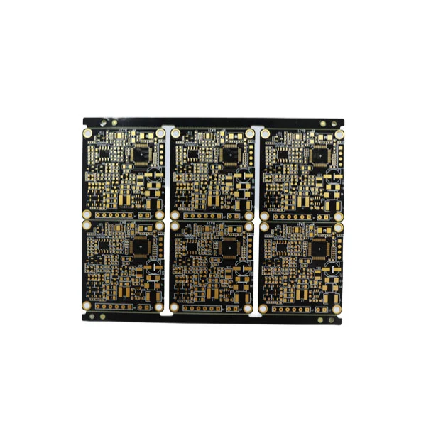
Understanding Printed Circuit Boards
A printed circuit board is an engineered platform that holds electronic components in position and connects them using conductive traces, copper planes, plated holes, and other features. Instead of relying on a separate wire for every connection, a PCB integrates many electrical pathways into a structured, compact assembly.
PCBs are used in devices ranging from simple LED lighting products to advanced communications equipment. Their layouts may be relatively straightforward or highly complex, depending on the electrical requirements, available space, and operating environment.
Key Components of a PCB
- Substrate: The base material provides mechanical support and electrical insulation.
- Copper traces: These conductive paths carry signals and power between components.
- Insulating layers: Dielectric materials separate conductive layers and help control electrical behavior.
- Solder mask: This protective coating helps prevent solder bridges and protects exposed copper, apart from intended openings.
- Silkscreen: Printed markings identify component positions, polarity, reference designators, and other assembly information.
- Vias and plated holes: These structures connect conductive layers or accommodate component leads, depending on their design.
How Does a PCB Work?
When power is applied, current flows through designed conductive paths, while signal traces transmit information between integrated circuits, sensors, connectors, and other components. The board layout determines how these connections are arranged and how electrical characteristics such as resistance, capacitance, inductance, and impedance affect circuit behavior.
A well-designed PCB does more than establish connectivity. It also supports heat management, reduces unwanted electrical interference, provides reliable mechanical mounting, and helps ensure that a product can be assembled consistently at scale.
Why PCB Quality Matters for Product Reliability
A circuit board can look acceptable and still contain defects that affect performance. Small changes in trace geometry, poor solderability, damaged plating, material inconsistency, or insufficient thermal design can cause intermittent faults or premature product failure.
For manufacturers, these issues can translate into rework, warranty claims, production delays, and dissatisfied customers. For engineering teams, they may require time-consuming debugging and another prototype cycle.
Electrical Performance
Appropriate trace widths, spacing, grounding, and impedance control help maintain stable signal transmission and current delivery.
Mechanical Durability
Suitable materials and board thickness help the assembly withstand handling, vibration, connector insertion, and normal operating stresses.
Thermal Management
Effective copper distribution, thermal vias, component placement, and material selection can reduce the risk of excessive heat buildup.
Manufacturing Consistency
Clear specifications and appropriate process controls reduce variation between production batches and support repeatable assembly.
Common Printed Circuit Board Types
Different applications require different PCB structures. The best choice depends on component density, routing complexity, electrical performance, mechanical constraints, and the available manufacturing budget.
| PCB Type | Main Characteristics | Typical Applications | Important Considerations |
|---|---|---|---|
| Single-sided PCB | Conductive copper on one side of the substrate | Basic controls, simple lighting, low-complexity electronics | Limited routing flexibility |
| Double-sided PCB | Copper layers on both sides, often connected through plated holes | Power supplies, appliances, industrial controls | Requires careful routing and layer connectivity |
| Multilayer PCB | Three or more conductive layers laminated together | Computing, networking, medical and industrial electronics | Stack-up, via structure, and fabrication complexity |
| Rigid PCB | Uses a rigid substrate to maintain its shape | Controllers, instruments, consumer electronics | Board outline, thickness, and mounting requirements |
| Flexible PCB | Uses flexible insulating materials for bending or compact routing | Wearables, cameras, compact assemblies | Bend radius, copper fatigue, and handling |
| Rigid-flex PCB | Combines rigid sections with flexible interconnections | Compact equipment with limited wiring space | Higher design and manufacturing complexity |
| Metal-core PCB | Uses a metal base to assist thermal transfer | LED lighting and selected power electronics | Thermal design and electrical isolation |
For straightforward products, a single- or double-sided board may be sufficient. High-density products may require multilayer construction, while space-constrained equipment can benefit from flexible or rigid-flex designs. Metal-core boards can be useful where heat dissipation is a major concern, but their suitability depends on the complete thermal and electrical design.
How Materials and Construction Affect PCB Performance
Material selection influences electrical insulation, mechanical strength, moisture resistance, thermal stability, and fabrication cost. Engineers should choose materials according to actual operating conditions instead of selecting a specification solely because it is commonly used.
FR-4 and Other Substrate Options
FR-4 is a widely used glass-reinforced epoxy laminate. It suits many general-purpose electronic products because it offers a practical balance of electrical properties, mechanical strength, availability, and cost. However, not every FR-4 grade has identical thermal or high-frequency characteristics.
High-speed or high-frequency designs may need laminates with more tightly controlled dielectric properties and lower signal loss. Flexible circuits commonly use polyimide-based materials, while metal-core constructions may be considered for applications that require a different approach to heat transfer.
Important Construction Parameters
- Board thickness: Must match enclosure clearances, connector geometry, stiffness requirements, and assembly constraints.
- Copper weight: Affects current-carrying capability, heat generation, and achievable trace geometry.
- Layer stack-up: Influences routing density, signal integrity, return paths, and manufacturing complexity.
- Surface finish: Must provide suitable solderability, storage performance, and compatibility with assembly requirements.
- Thermal properties: Matter when components generate substantial heat or experience repeated temperature changes.
- Operating environment: Humidity, vibration, chemicals, and temperature extremes may require specific materials or protective measures.
Surface finishes such as lead-free hot-air solder leveling, immersion tin, immersion silver, and electroless nickel immersion gold have different characteristics and process considerations. The choice should reflect component pitch, assembly method, storage needs, environmental requirements, and supplier capability.
Essential PCB Design Considerations Before Production
Manufacturing problems often begin before fabrication. An incomplete design package, unrealistic tolerances, insufficient spacing, or unclear revision information can create avoidable delays. Early collaboration between the design team and manufacturer helps identify these risks before they affect the schedule.
1. Confirm Electrical Requirements
Define operating voltage, expected current, signal frequency, impedance requirements, grounding strategy, and noise sensitivity. Trace widths and spacing should be calculated or validated against the relevant electrical, thermal, and fabrication constraints rather than selected by guesswork.
2. Plan Component Placement and Routing
Place critical components with signal paths, power distribution, heat sources, connectors, and service access in mind. High-speed circuits may require controlled impedance and continuous return paths. Sensitive analog signals may need separation from noisy switching circuits.
3. Check Thermal and Mechanical Constraints
Confirm mounting holes, board outline, enclosure clearances, component heights, connector positions, and expected mechanical loads. Consider airflow, heat spreaders, copper planes, and thermal vias where appropriate. Do not assume that a thicker board or more copper will automatically solve every thermal problem.
4. Design for Manufacturability
Review minimum trace width and spacing, drill sizes, annular rings, solder-mask clearances, copper-to-edge distances, and panelization requirements against the intended fabricator's capabilities. The actual acceptable limits depend on material, layer count, board size, production process, and yield expectations.
5. Prepare a Complete Data Package
Depending on the product and service scope, a release package may include Gerber or other accepted fabrication data, NC drill files, board stack-up details, fabrication notes, board outline, bill of materials, assembly drawings, pick-and-place files, and test requirements. Confirm the required file formats with the supplier before release.
How the PCB Manufacturing Process Works
PCB fabrication involves multiple controlled steps. The exact sequence varies with board construction, layer count, materials, and production technology, but the following overview illustrates the main stages for many rigid printed circuit boards.
- Engineering review: The manufacturer reviews the design data, specifications, material requirements, and manufacturing feasibility.
- Material preparation: Laminate and copper-clad materials are selected and prepared according to the board construction.
- Pattern formation: Imaging and etching processes define the required conductive circuitry on copper layers.
- Layer alignment and lamination: For multilayer boards, inner layers are aligned and bonded with insulating materials under controlled conditions.
- Drilling and via formation: Holes are created for component leads or interlayer connections, with plated holes formed where specified.
- Outer-layer processing: Outer copper patterns are formed and processed according to the manufacturing flow.
- Solder mask and markings: Protective coatings and identification markings are applied as required.
- Surface finishing: Exposed pads receive the specified finish to support the intended connection or soldering process.
- Profiling: The board outline and any specified slots or cutouts are produced.
- Inspection and electrical testing: The finished boards are checked against applicable acceptance requirements.
- Packaging and shipment: Accepted boards are packed to help prevent handling, moisture, and transport damage.
When component assembly is included, additional stages may involve solder-paste printing, component placement, reflow soldering, through-hole soldering, cleaning where required, inspection, and functional testing. Bare-board fabrication and PCB assembly are related but distinct services, so buyers should confirm exactly what their quotation includes.
Testing and Quality Control for Printed Circuit Boards
Quality control should match the product's risks and documented acceptance criteria. No single inspection method can identify every possible defect, which is why manufacturers often combine visual checks, dimensional verification, electrical testing, and specialized inspection methods.
| Inspection Method | Purpose | What Buyers Should Confirm |
|---|---|---|
| Visual inspection | Identifies visible surface, marking, finish, and workmanship issues | Acceptance criteria and inspection coverage |
| Automated optical inspection (AOI) | Checks image-based circuit patterns for specified defects | Which layers or features are inspected and how results are handled |
| Electrical continuity and isolation testing | Checks intended connections and unintended shorts against the test data | Test coverage, netlist accuracy, and applicable acceptance limits |
| X-ray inspection | Helps examine internal structures that are not directly visible | Whether the board construction or identified risk warrants this method |
| Dimensional inspection | Verifies specified dimensions, holes, slots, and board outline | Critical dimensions and measurement tolerances |
| Microsection analysis | Examines internal construction, plating, and selected structural details | Whether required by the specification, qualification plan, or risk level |
For higher-reliability applications, discuss applicable industry standards, material traceability, process documentation, lot identification, change control, and any additional qualification tests. Standards and certification requirements should be selected according to the product's intended use; they should not be assumed to apply automatically to every PCB.
It is also useful to establish a clear process for reporting nonconformities. Ask how defects are documented, how affected lots are contained, how corrective actions are verified, and how engineering changes are approved before production resumes.
Where Printed Circuit Boards Are Used
PCBs are central to almost every category of modern electronic equipment. Each application presents a different combination of performance, cost, environmental, and reliability requirements.
Consumer Electronics
Smart devices, home appliances, audio equipment, and personal electronics require compact layouts, consistent production, and effective integration of control, power, and communication circuits.
Industrial Automation
Motor controllers, sensors, programmable control systems, and monitoring equipment may need robust construction, stable operation, noise management, and resistance to demanding industrial environments.
Telecommunications and Networking
Communication systems often place greater emphasis on signal integrity, impedance control, low-loss materials, dense routing, and carefully planned grounding and return paths.
Automotive Electronics
Automotive applications can experience vibration, temperature variation, and long service-life expectations. Board design, material selection, assembly controls, and qualification must align with the specific system's requirements.
Medical and Measurement Equipment
Boards used in medical or precision measurement products may require documented traceability, controlled manufacturing processes, and verification appropriate to the equipment's intended function and applicable regulations.
LED and Power Electronics
Lighting drivers and power conversion systems must address current handling, switching noise, component spacing, insulation, and heat dissipation. The appropriate PCB construction depends on power density and the overall thermal design.
Factors That Influence Printed Circuit Board Cost
PCB pricing reflects more than the physical size of the board. Production complexity, material availability, processing time, inspection requirements, and order quantity can all affect the final quotation.
- Layer count: More layers generally require additional processing and more complex alignment and lamination.
- Material choice: Specialized high-frequency, high-temperature, or flexible materials may cost more than standard materials.
- Board dimensions: Size affects material usage, panel utilization, handling, and production yield.
- Design complexity: Fine features, dense routing, special drilling, blind or buried vias, and tight tolerances may increase processing difficulty.
- Copper requirements: Heavy copper or other specialized copper specifications can influence processing and cost.
- Surface finish: Different finishes have different material, process, and handling costs.
- Order quantity: Engineering setup and tooling costs may be distributed across more units in larger orders, depending on the supplier's pricing model.
- Inspection and documentation: Enhanced testing, qualification, traceability, and reporting may add cost but can be necessary for the application.
- Lead time: Expedited production may carry additional charges and depends on actual material and factory capacity.
How to Reduce Cost Without Creating New Risks
Start by removing unnecessary complexity rather than simply requesting lower prices. Review whether the design truly requires every layer, special via type, tolerance, or finish. Improve panel utilization where practical, standardize materials across product families when technically suitable, and provide complete manufacturing data to reduce clarification cycles.
For prototypes, consider whether a staged validation plan can identify design issues before a larger order is released. For volume production, evaluate total landed cost, expected yield, quality performance, and delivery reliability rather than unit price alone.
How to Choose a Reliable Printed Circuit Board Supplier
A capable supplier should be able to explain its manufacturing capabilities, review technical requirements, communicate risks, and provide quality information appropriate to the project. The goal is not simply to find a factory that can produce a board, but to establish a dependable process from quotation through repeat orders.
Review Technical Capability
Ask about supported layer counts, material types, board dimensions, copper thicknesses, minimum feature capabilities, drill limits, surface finishes, and tolerances. Request confirmation that the supplier can meet the actual specifications of your design. General capability statements should be verified against the requirements of the particular job.
Evaluate Communication and Engineering Support
Clear communication is especially important when a design contains unusual requirements or incomplete information. A supplier should raise manufacturability questions, identify conflicting specifications, and confirm proposed changes before proceeding.
Understand Quality Systems and Documentation
Discuss inspection methods, electrical test coverage, traceability, nonconformance handling, change control, and relevant certifications. Confirm the scope and validity of any certification that is important to your industry or customer contract.
Check Delivery and Order Management
Ask for a realistic lead-time estimate, including engineering review, material procurement, fabrication, inspection, and shipping. For recurring production, discuss forecast planning, revision management, packaging, and the process for handling urgent requirements.
Compare Quotations on the Same Basis
Two quotations are not directly comparable if they use different materials, finishes, testing methods, tolerances, or delivery terms. Provide all potential suppliers with the same released data package and request written confirmation of the included specifications and services.
When evaluating manufacturers, Fanway can be included in your supplier research. Share your board requirements and project details to establish whether the available capabilities, quality processes, and service scope match your needs.
Printed Circuit Board Pre-Order Checklist
Use the following checklist before requesting a quotation or approving a production run. A complete request helps reduce misunderstandings and makes supplier quotations easier to compare.
- Confirm the final board outline, dimensions, thickness, and required quantity.
- Specify the number of copper layers and approved stack-up.
- Identify the substrate material and any electrical or thermal requirements.
- Define copper thickness, surface finish, solder mask, and silkscreen requirements.
- Provide current fabrication data, drill files, and any required drawings or notes.
- State critical tolerances, impedance requirements, and special via structures.
- Identify operating temperature, humidity, vibration, or other environmental conditions.
- Define inspection, electrical testing, documentation, and acceptance requirements.
- Confirm whether the order covers bare-board fabrication, component assembly, or both.
- Agree on the released revision, production schedule, packaging, and delivery terms.
- Clarify how engineering changes, nonconforming boards, and repeat orders will be managed.
If some requirements are still undecided, identify them clearly rather than leaving them implicit. Your engineering team and supplier can then determine which details must be finalized before production and which can be resolved during a formal design review.
Frequently Asked Questions About Printed Circuit Boards
1. What is the main purpose of a printed circuit board?
A PCB supports electronic components and connects them through conductive pathways. It provides an organized structure for distributing power and transmitting signals while helping the electronic assembly meet mechanical and environmental requirements.
2. What is the difference between a PCB and a PCBA?
A PCB generally refers to the fabricated circuit board before components are installed. A PCBA, or printed circuit board assembly, is a board populated with electronic components and assembled using the required soldering and inspection processes. A supplier may offer fabrication, assembly, or an integrated service covering both.
3. Which PCB type is best for a new electronic product?
There is no single best type for every product. The choice depends on circuit complexity, available space, operating frequency, current, thermal conditions, mechanical requirements, and cost. Simple products may use single- or double-sided boards, while dense or high-performance designs may require multilayer construction.
4. Why are multilayer PCBs more complex to manufacture?
Multilayer boards require precise alignment and bonding of multiple conductive layers. Their fabrication may also involve more complex drilling, plating, stack-up control, inspection, and electrical testing. These additional steps can increase manufacturing time and cost.
5. Which files are needed to manufacture a PCB?
Common requirements include Gerber or another accepted fabrication data format, drill files, a board outline, and fabrication notes. Multilayer or specialized boards may also require stack-up information, impedance details, material specifications, and additional drawings. Assembly orders generally need a bill of materials, pick-and-place data, and assembly documentation as well.
6. How can I improve PCB reliability?
Use materials appropriate for the operating environment, validate electrical and thermal design, follow the fabricator's design rules, maintain accurate revision control, and define suitable inspection and testing requirements. Reliability also depends on component selection, assembly quality, enclosure design, and the product's actual operating conditions.
7. What causes PCB manufacturing delays?
Common causes include incomplete design files, inconsistent revisions, unavailable materials, unclear tolerances, design-rule conflicts, special processing requirements, and late engineering changes. Providing complete data and resolving technical questions early can help reduce avoidable delays.
8. How can I compare PCB manufacturer quotations fairly?
Compare quotations using the same board data, quantity, material, copper specification, layer count, surface finish, tolerances, testing requirements, delivery terms, and assembly scope. Also evaluate communication quality, process documentation, and the supplier's ability to support repeat orders.
9. Does a higher layer count always mean better performance?
No. More layers can improve routing flexibility and provide dedicated planes, but they also add complexity and cost. Performance depends on the complete design, including stack-up, component placement, routing, grounding, material properties, and manufacturing quality.
10. What information should I provide when requesting a PCB quote?
Provide the fabrication files, board dimensions, layer count, material and copper requirements, surface finish, quantity, tolerances, testing needs, target delivery date, and shipping destination. If assembly is required, also include the bill of materials, assembly files, component sourcing preferences, and inspection expectations.
Build Better Electronic Products with the Right PCB Decisions
A printed circuit board is much more than a physical base for electronic components. Its material, layer structure, circuit layout, manufacturing precision, and quality controls all contribute to the performance and service life of the finished product. Selecting the right board begins with a clear understanding of electrical requirements, mechanical constraints, environmental conditions, and production objectives.
By preparing complete design data, confirming manufacturing capabilities, defining inspection requirements, and comparing quotations on an equivalent basis, engineering and procurement teams can reduce avoidable risks and improve production planning. Early communication between the product designer and the PCB manufacturer is especially valuable when the design involves tight tolerances, high-speed signals, demanding thermal conditions, or complex multilayer construction.
Looking for a PCB Manufacturing Partner?
Whether you are developing a prototype, improving an existing circuit board, or preparing for volume production, clear technical communication is the first step toward a successful project. Visit Fanway to learn more about its PCB-related services and discuss your project requirements. Share your board specifications, production quantity, and target schedule to help determine the most suitable next steps.
Have questions about your next printed circuit board project? Contact us to discuss your requirements, request a quotation, and explore a practical path from design data to dependable production.
Visit Fanway