

What Makes a High-Quality Printed Circuit Board Essential for Modern Electronics?
2025-08-05
In today’s digital age, electronic devices have become integral to nearly every aspect of human life. From the smartphones we carry in our pockets to the complex medical equipment saving lives in hospitals, from the aerospace technology exploring the skies to the smart home systems making our lives more convenient—all these devices share a common foundational component: the printed circuit board (PCB). As the backbone of electronic devices, the quality, design, and performance of a printed circuit board directly impact the functionality, reliability, and longevity of the end product. But what exactly defines a high-quality printed circuit board, and why is it so essential in modern electronics? In this comprehensive guide, we’ll delve into the world of printed circuit boards, exploring their characteristics, manufacturing processes, key parameters, and answering common questions to help you understand their critical role.
Trending News Headlines: Hot Topics in Printed Circuit Boards
- "Flexible Printed Circuit Boards: Revolutionizing Wearable Technology Design"
- "High-Temperature Printed Circuit Boards: Meeting Automotive and Aerospace Demands"
- "Eco-Friendly Printed Circuit Boards: Sustainable Materials Gain Traction"
- "Miniaturized Printed Circuit Boards: Powering the Next Generation of IoT Devices"
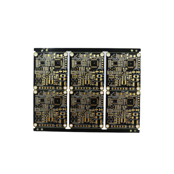
What Is a Printed Circuit Board and Its Core Functions?
What Defines a High-Quality Printed Circuit Board?
Superior Material Selection
The substrate material is the foundation of a printed circuit board, and choosing the right material is crucial. High-quality printed circuit boards use substrates with excellent dielectric properties, high thermal conductivity, and good mechanical strength. Common materials include FR-4 (a glass-reinforced epoxy laminate), which is widely used for general-purpose applications. For high-performance devices, materials like polyimide (for flexible PCBs), aluminum (for heat dissipation), or PTFE (Teflon) for high-frequency applications are preferred. The copper used for traces should be of high purity to ensure low electrical resistance and efficient signal transmission.
Precise Design and Manufacturing
A well-designed printed circuit board layout is essential for minimizing signal interference, optimizing power distribution, and ensuring efficient heat management. High-quality printed circuit boards are designed using advanced CAD software, with careful attention to trace routing, component placement, and layer stacking. The manufacturing process must adhere to strict tolerances to ensure that traces are of the correct width and thickness, holes are drilled accurately, and surface finishes are applied uniformly.
Reliability and Durability
High-quality printed circuit boards are built to withstand harsh environmental conditions, including temperature fluctuations, humidity, vibration, and chemical exposure. They undergo rigorous testing to ensure that they can perform consistently over an extended period, reducing the risk of device failure and minimizing maintenance costs. For example, in automotive applications, printed circuit boards must endure extreme temperatures ranging from -40°C to 125°C, while in aerospace applications, they must withstand high levels of vibration and radiation.
Compliance with Industry Standards
How Are High-Quality Printed Circuit Boards Manufactured?
Design and Prototyping
The process begins with the design of the printed circuit board using specialized PCB design software. Engineers create a schematic diagram of the circuit, which is then converted into a layout that specifies the placement of components and the routing of traces. Once the design is finalized, a prototype is manufactured to test the functionality and performance of the board. Prototyping allows for any design flaws to be identified and corrected before mass production.
Substrate Preparation
The substrate material (usually FR-4 or another laminate) is cut to the required size and cleaned to remove any contaminants that could affect the bonding of copper. The substrate is then coated with a thin layer of copper foil, which will form the conductive traces.
Imaging and Etching
A photosensitive material (photoresist) is applied to the copper-clad substrate. The PCB design is then transferred onto the photoresist using a UV light source, creating a pattern that corresponds to the desired traces. The unexposed areas of the photoresist are removed, leaving the copper that will form the traces protected. The substrate is then immersed in an etching solution, which removes the unprotected copper, leaving behind the conductive traces.
Drilling
Holes are drilled into the printed circuit board to allow for the insertion of through-hole components and to create vias (connections between different layers of a multi-layer board). The drilling process uses high-precision drills to ensure that holes are of the correct size and position.
Plating
The drilled holes are plated with copper to create electrical connections between different layers of the board. This process, known as electroplating, ensures that the vias and through-holes are conductive.
Surface Finishing
A surface finish is applied to the printed circuit board to protect the copper traces from oxidation, improve solderability, and enhance durability. Common surface finishes include HASL (Hot Air Solder Leveling), ENIG (Electroless Nickel Immersion Gold), OSP (Organic Solderability Preservative), and immersion silver.
Testing and Inspection
Our Printed Circuit Board Specifications
|
Parameter
|
Standard PCB
|
Flexible PCB
|
High-Frequency PCB
|
Aluminum PCB
|
|
Substrate Material
|
FR-4 (Glass Epoxy)
|
Polyimide
|
PTFE, Rogers
|
Aluminum with FR-4 overlay
|
|
Number of Layers
|
2 - 24 layers
|
1 - 10 layers
|
2 - 16 layers
|
1 - 4 layers
|
|
Board Thickness
|
0.2mm - 3.2mm
|
0.05mm - 0.5mm
|
0.2mm - 2.0mm
|
0.8mm - 3.0mm (aluminum base: 0.5mm - 2.0mm)
|
|
Copper Thickness
|
1oz - 10oz
|
0.5oz - 3oz
|
1oz - 5oz
|
1oz - 8oz
|
|
Minimum Trace Width/Spacing
|
3mil/3mil
|
5mil/5mil
|
2mil/2mil
|
4mil/4mil
|
|
Minimum Hole Size
|
0.2mm
|
0.3mm
|
0.15mm
|
0.25mm
|
|
Maximum Board Size
|
1200mm x 600mm
|
500mm x 300mm
|
800mm x 600mm
|
1000mm x 600mm
|
|
Surface Finish Options
|
HASL, ENIG, OSP, Immersion Silver
|
ENIG, Immersion Tin
|
ENIG, Silver
|
ENIG, HASL
|
|
Operating Temperature Range
|
-40°C to 125°C
|
-55°C to 150°C
|
-55°C to 125°C
|
-40°C to 170°C
|
|
Certifications
|
ISO 9001, IPC-A-600 Class 2
|
ISO 9001, IPC-A-600 Class 2
|
ISO 9001, IPC-A-600 Class 3
|
ISO 9001, IPC-A-600 Class 2, IATF 16949
|
FAQ: Common Questions About Printed Circuit Boards
Q: What are the main differences between single-layer, double-layer, and multi-layer printed circuit boards?
A: Single-layer printed circuit boards have conductive traces on only one side of the substrate. They are simple in design, cost-effective, and suitable for basic electronic devices such as calculators, radios, and simple sensors. Double-layer printed circuit boards have traces on both sides of the substrate, with vias (holes) connecting the traces on each side. They offer more flexibility in design and are used in devices such as power supplies, amplifiers, and industrial controls. Multi-layer printed circuit boards consist of three or more layers of conductive traces separated by insulating substrate material, connected via vias. They provide a high density of connections, allowing for complex circuit designs, and are used in advanced devices such as smartphones, computers, medical equipment, and aerospace systems. The number of layers depends on the complexity of the circuit, with more layers enabling more components and connections in a smaller space.
Q: How do I determine the right printed circuit board material for my application?
A: Choosing the right printed circuit board material depends on several factors related to your application. First, consider the operating environment: if the device will be exposed to high temperatures (such as in automotive or industrial applications), materials with high thermal resistance like aluminum or polyimide are suitable. For flexible devices (such as wearables), polyimide-based flexible PCBs are ideal. Second, consider the electrical requirements: high-frequency applications (such as 5G equipment or radar systems) require materials with low dielectric constant and loss, such as PTFE or Rogers materials. For general-purpose applications with moderate electrical demands, FR-4 is a cost-effective choice. Third, consider mechanical requirements: if the device needs to be lightweight or resistant to vibration, materials with good mechanical strength and flexibility are important. Additionally, factors such as cost, manufacturing complexity, and compliance with industry standards should also be taken into account. Consulting with a printed circuit board manufacturer can help you select the most appropriate material based on your specific needs.