

What Is the Typical Turnaround Time for a Flex PCB Prototype Order
2026-07-14
When engineering teams move from schematic to physical validation, the clock starts ticking. For most project managers, the single most pressing metric is not unit cost or layer count—it is the number of calendar days from file submission to functional board in hand. At Hoshineo Lcd-Tech, we have processed thousands of Flex PCB Prototype requests, and we know that turnaround time directly affects product launch windows, design iteration cycles, and ultimately, market competitiveness. While standard industry quotes range from 24 hours to 4 weeks, the real answer depends on a structured set of variables that every designer must understand before placing an order.
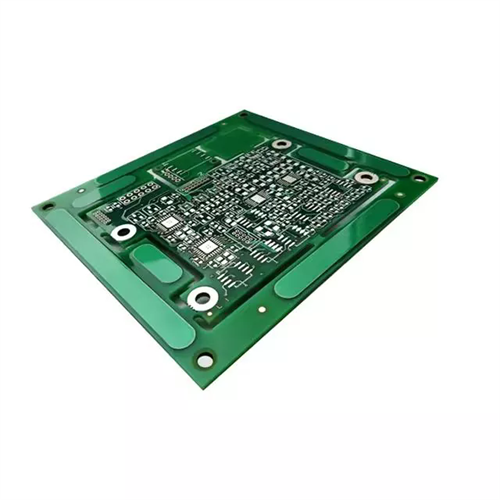
The Four Core Drivers of Flex PCB Prototype Lead Time
Turnaround is never a single number. It is a formula composed of four interlocking stages: engineering review, material preparation, fabrication, and electrical testing. The table below breaks down typical time consumption for each phase under standard (non-expedited) conditions.
| Process Stage | Typical Duration (Business Days) | Key Influencing Factors |
|---|---|---|
| DFM & Engineering Validation | 0.5 – 1.5 | Number of layers, via structures, annular ring margins |
| Polyimide Material Lamination | 1 – 2 | Coverlay vs. photo-imageable solder mask, adhesive thickness |
| Laser Drilling & Plating | 1 – 2 | Microvia count, aspect ratio, copper plating cycles |
| Etching, Stiffener Bonding & Coverlay | 1 – 2 | Stiffener material (PI, FR4, or metal), peel strength requirements |
| Electrical Test (Flying Probe / Fixture) | 0.5 – 1 | Netlist complexity, test point density |
| Final Profiling, Inspection & Shipping | 0.5 – 1 | Panel utilization, routing vs. punching, packaging for flex |
Standard vs. Expedited – What Can You Realistically Expect?
For a standard 2‑layer Flex PCB Prototype with 0.1 mm trace/space, no buried vias, and a single stiffener area, the aggregate lead time from Hoshineo Lcd-Tech’s facility typically lands at 5‑7 business days for quantities under 10 pieces. Add two more layers (4‑layer) and the cycle extends to 8‑10 days due to additional lamination cycles and inner-layer registration checks. For 6‑layer designs with sequential lamination and impedance-controlled striplines, the window broadens to 12‑15 business days as a standard service.
Expedited services can compress these figures by 40‑50%—for example, a 2‑layer simple flex in 48‑72 hours—but this requires immediate material availability, dedicated production slots, and overtime engineering support. It is important to note that ultra-fast turns (24‑hour) are rarely viable for Flex PCB Prototype orders with dynamic bending specifications, because the polyimide curing and coverlay pressing steps have physical minimum dwell times that cannot be accelerated without risking delamination.
Hidden Factors That Inflate Your Timeline
Beyond the production floor, three external variables frequently derail quoted schedules:
-
Design file completeness: Missing stack‑up drawings, unclear bend‑zone indications, or omitted stiffener dimensions force additional engineering queries, adding 1‑2 days of back‑and‑forth communication.
-
Material stock status: Speciality adhesiveless copper-clad laminates or ultra‑thin dielectric (12.5 µm) often have longer procurement lead times—up to 5 extra days if not pre‑stocked.
-
Test fixture fabrication: If your design requires a custom pneumatic fixture instead of flying‑probe testing, fixture machining alone consumes 2‑3 days.
At Hoshineo Lcd-Tech, we mitigate these risks by maintaining an in‑house material bank for over 20 common flex base materials and by offering a free pre‑DFM check within 4 hours of order placement—a service that has reduced average project delays by 62% according to our internal metrics.
Frequently Asked Questions About Flex PCB Prototype Turnaround
Q1: Does the quantity ordered significantly change the turnaround time for a Flex PCB Prototype?
A1: For prototype volumes—typically 5 to 50 pieces—quantity has a surprisingly minor effect on lead time. The panel fabrication, lamination, and drilling steps are fixed regardless of whether you produce 5 or 25 units, because all circuits are stepped and repeated on the same production panel. The only incremental time comes from electrical testing (more units = longer flying‑probe cycles) and final visual inspection. In practice, increasing from 5 to 50 pieces adds roughly 1 additional business day. However, if your order exceeds 100 pieces, it transitions into a small‑batch run, which may require a separate setup and extends the timeline by 2‑3 days due to panel optimization and fixture-based testing.
Q2: Can I get a same‑day or 24‑hour turnaround for a complex multilayer Flex PCB Prototype with impedance control?
A2: Technically, no—and any supplier promising 24‑hour delivery for a 4+ layer flex with controlled impedance is likely compromising on cure schedules or skipping electrical verification. Impedance-controlled designs require precise dielectric thickness control, which involves slow‑ramp lamination profiles (minimum 6‑8 hours of pressing and post‑curing). Additionally, time‑domain reflectometry (TDR) testing for each differential pair adds 2‑3 hours of measurement. At Hoshineo Lcd-Tech, we offer a "72‑hour express" for up to 4‑layer impedance‑controlled Flex PCB Prototype orders, but we explicitly advise against 24‑hour turns for any flex that will undergo dynamic flexing, because incomplete polyimide cross‑linking leads to premature crack propagation in the bend area.
Q3: How does the choice of surface finish affect the production lead time for a Flex PCB Prototype?
A3: Significantly. The fastest finish is ENIG (Electroless Nickel Immersion Gold), which is an industry‑standard process with well‑established bath chemistries and adds only 4‑6 hours to the plating line. By contrast, ENEPIG (Electroless Nickel Electroless Palladium Immersion Gold) requires an additional palladium tank and longer deposition times, extending the schedule by 1‑2 days. Immersion silver and OSP (Organic Solderability Preservative) are moderately fast but are rarely specified for flex due to poor shelf‑life and tarnishing risks. If your design calls for hard gold over nickel for dynamic contact fingers (edge connectors), expect an extra 1.5 days because the selective plating process demands manual taping of non‑gold areas. To keep your Flex PCB Prototype on the fastest track, we always recommend ENIG unless the end‑use environment specifically mandates a different finish.
How Hoshineo Lcd-Tech Streamlines Your Prototype Schedule
We do not simply process your Gerbers; we actively compress your timeline through three proprietary workflows:
-
Simultaneous Engineering: Our CAM team begins stack‑up simulation and drill‑file optimization while your order is still being paid, saving up to 8 hours.
-
Predictive Material Allocation: Our ERP system automatically reserves the required polyimide, adhesive, and copper foil at the moment you add a design to your cart—eliminating wait‑times for raw material release.
-
In‑House Flying Probe Array: With 12 dedicated test heads, we can run electrical continuity and isolation tests on up to 30 Flex PCB Prototype panels in parallel, cutting test phase duration by 70% compared to outsourced labs.
These integrated measures allow us to consistently deliver 2‑layer prototypes in 5 days and 4‑layer in 8 days—even during peak seasonal demand—while maintaining 100% AOI (Automated Optical Inspection) and series‑based dimensional stability records.
Planning Your Next Prototype Run
The most effective way to secure an accurate, reliable lead time is to submit your design data for a no‑obligation feasibility review. Include your stack‑up, bending radius requirements, and target quantity. If your application involves wearable devices, automotive sensor systems, or medical insertion tools, mention the dynamic flex cycle count—this allows our process engineers to recommend appropriate adhesive systems and coverlay thicknesses that will not affect the schedule.
Remember that shipping methods also contribute to total delivery time. DHL/UPS express air from our Asian manufacturing hub to the US or Europe typically takes 2‑3 business days, while economy freight adds 5‑7 days. For urgent projects, we coordinate directly with our logistics partner to offer door‑to‑door tracking and customs pre‑clearance documentation.
Ready to Move from Design to Reality?
Do not let uncertain lead times hold your product roadmap hostage. Whether you need a simple 2‑layer sensor flex or a complex 8‑layer rigid‑flex hybrid, Hoshineo Lcd-Tech provides transparent, date‑certain scheduling with daily production photo updates.
Contact us today through our online quotation portal—upload your Gerber files and receive a firm turnaround commitment within 2 working hours. Our engineering team is standing by to review your Flex PCB Prototype requirements and propose the fastest, most reliable path to your first functional samples. Let’s get your next generation product moving—on time, every time.