

What Is a Double Layer PCB?
2026-01-28
In modern electronics manufacturing, the demand for compact design, stable performance, and cost efficiency continues to grow. As a result, Double Layer PCB has become one of the most widely used circuit board solutions across multiple industries. Compared with single-sided boards, it offers greater flexibility in circuit design while maintaining a reasonable production cost, making it an ideal balance between performance and affordability for many applications.
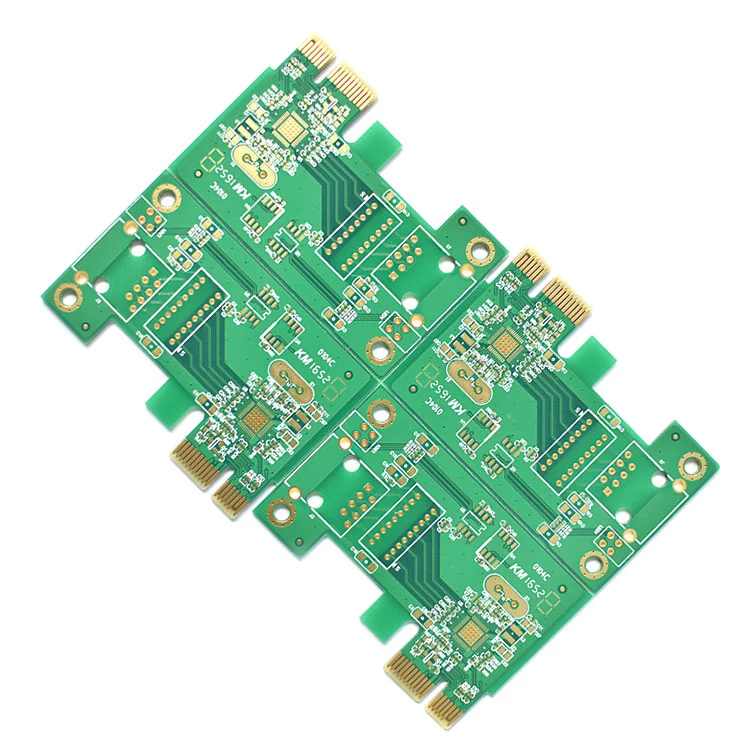
A Double Layer PCB refers to a printed circuit board that has conductive copper layers on both sides of the substrate, allowing components and signal routing on the top and bottom layers. This structure significantly improves circuit density and functionality without the complexity of multilayer PCBs.
Why Choose Double Layer PCB Instead of Single Layer PCB?
When comparing Single Layer PCB vs Double Layer PCB, the advantages of double-layer design become clear.
Key Differences at a Glance
| Feature | Single Layer PCB | Double Layer PCB |
|---|---|---|
| Circuit Density | Low | Medium to High |
| Wiring Flexibility | Limited | More flexible |
| Component Placement | One side only | Both sides |
| Cost | Lower | Moderate |
| Application Scope | Simple devices | Complex electronics |
For products that require moderate complexity, stable signal transmission, and compact layout, Double Layer PCB offers a superior solution without the higher cost of multilayer boards.
How Does a Double Layer PCB Work?
A Double Layer PCB works by connecting the top and bottom copper layers through vias, which allow electrical signals to pass between layers. This design enables engineers to:
-
Optimize routing paths
-
Reduce electromagnetic interference
-
Improve signal integrity
-
Enhance overall circuit reliability
At Shenzhen Fanway Technology Co., Ltd, advanced drilling and plating processes ensure strong via connections and consistent electrical performance.
What Are the Main Functions of Double Layer PCB?
The primary functions of a Double Layer PCB include:
-
Supporting complex circuit designs
-
Enhancing electrical performance
-
Improving space utilization
-
Providing stable mechanical support
These functions make Double Layer PCB a key component in consumer electronics, industrial control systems, communication devices, and power equipment.
What Is the Practical Effect of Using Double Layer PCB?
Using a Double Layer PCB leads to noticeable improvements in product performance:
-
Higher reliability in long-term operation
-
Reduced signal loss and noise
-
Smaller product size with more features
-
Better thermal distribution
Manufacturers can achieve higher production efficiency while end users benefit from more stable and durable electronic products.
Why Is Double Layer PCB Important in Modern Electronics?
As electronic devices become smaller and smarter, the limitations of single-layer boards are increasingly evident. Double Layer PCB plays a critical role by offering:
-
A scalable design foundation
-
Cost-effective performance improvement
-
Compatibility with automated assembly
-
Greater design freedom for engineers
This importance makes it one of the most commonly selected PCB types in today's global electronics market.
Why Choose Shenzhen Fanway Technology Co., Ltd for Double Layer PCB?
Shenzhen Fanway Technology Co., Ltd specializes in high-quality PCB manufacturing, providing customized Double Layer PCB solutions with:
-
Strict quality control standards
-
Advanced manufacturing equipment
-
Stable lead times
-
Professional engineering support
Our team understands both technical requirements and market demands, ensuring that every Double Layer PCB delivers reliable performance and commercial value.
Conclusion
Whether for consumer electronics or industrial applications, Double Layer PCB remains a practical and powerful solution that balances performance, complexity, and cost. Choosing the right PCB partner is just as important as choosing the right PCB structure.
If you are looking for a reliable manufacturer with strong technical expertise and flexible production capability, Shenzhen Fanway Technology Co., Ltd is ready to support your project.
👉 Contact us today to discuss your Double Layer PCB requirements and turn your ideas into high-performance electronic solutions.