

What Are The Latest Trends In HDI PCB Manufacturing Technology
2026-01-29
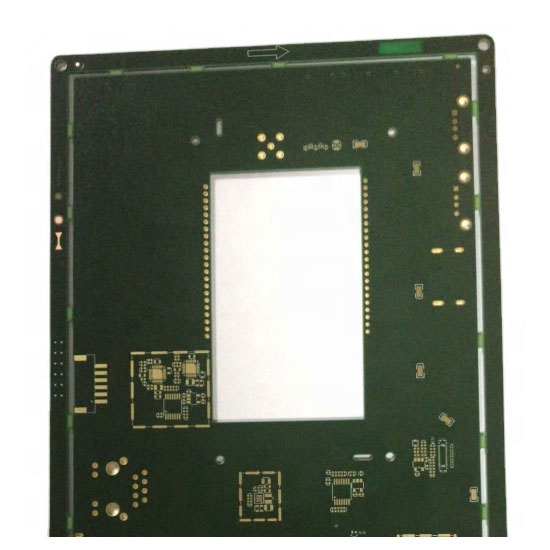
The landscape of modern electronics is defined by demands for higher speed, greater functionality, and smaller form factors. At the heart of this evolution lies HDI PCB (High-Density Interconnect Printed Circuit Board) technology. As a leader in advanced circuit solutions, Akeson is at the forefront of integrating the latest manufacturing trends to deliver unparalleled performance and reliability. Staying ahead of these innovations is crucial for developing cutting-edge products in sectors like 5G, IoT, and wearable technology.
Several key trends are currently shaping HDI PCB manufacturing:
-
Advanced Via-in-Pad and Microvia Technologies: The use of filled and capped microvias directly in component pads is becoming standard. This allows for finer pitch BGA routing and significantly improved signal integrity by shortening the path.
-
Any-Layer HDI (ELIC): Moving beyond 1+N+1 or 2+N+2 stack-ups, any-layer HDI PCB construction allows microvias to connect any layer to any other layer. This provides maximum routing density and design flexibility for the most complex, space-constrained devices.
-
Adoption of High-Frequency Materials: To support mmWave and high-speed digital applications, there is a growing shift toward specialized laminate materials with low dielectric constant (Dk) and dissipation factor (Df).
-
Increased Automation and AI in DFM: Design for Manufacturability (DFM) checks are now leveraging artificial intelligence to predict potential production issues, optimize panel utilization, and enhance yield rates automatically.
The following table compares traditional and trending HDI PCB features:
| Feature | Traditional Approach | Latest Trend |
|---|---|---|
| Via Structure | Through-hole vias, blind/buried vias | Any-layer microvias, via-in-pad |
| Line/Space | 3/3 mil or larger | Sub-2/2 mil becoming common |
| Material Core | Standard FR-4 | High-speed/low-loss laminates (e.g., Megtron, Tachyon) |
| Design Driver | Connectivity | Signal Integrity & Thermal Management |
HDI PCB FAQ
What is the primary advantage of an HDI PCB over a standard PCB?
The primary advantage is superior component density and miniaturization capability. HDI PCBs utilize finer lines, microvias, and advanced stack-ups to route more connections in a much smaller area, enabling the sleek, powerful devices we use today.
How does HDI technology improve signal performance?
It improves performance by drastically reducing signal path lengths and parasitic inductance/capacitance through the use of microvias. Shorter pathways mean faster signal transmission, less power loss, and reduced noise and cross-talk, which is critical for high-frequency applications.
Are HDI PCBs more expensive to manufacture?
Initially, yes, due to complex processes and specialized equipment. However, the overall system cost can be lower. An HDI PCB often consolidates what would require multiple standard boards into one, reducing assembly steps, improving reliability, and enabling a smaller, more marketable end product, offering excellent value.
To leverage these cutting-edge trends for your next project, you need a partner with proven expertise and advanced capabilities. Akeson provides end-to-end solutions, from design support utilizing the latest any-layer techniques to precision manufacturing with high-frequency materials. Our engineering team ensures your HDI PCB is not just built, but optimized for performance, reliability, and cost-effectiveness.
Contact us today to discuss how our HDI PCB manufacturing expertise can bring your innovative electronic designs to life.