

What Are the Latest Advancements in HDI PCB Materials and Processes
2026-01-14
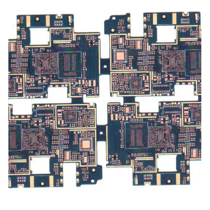
In the fast-evolving world of electronics, staying ahead means pushing the boundaries of HDI PCB technology. The relentless drive for smaller, faster, and more reliable devices has fueled significant innovation at the material and process levels. At Akeson, we specialize in integrating these cutting-edge advancements to deliver superior HDI PCB solutions that meet the rigorous demands of modern applications, from 5G infrastructure to advanced medical devices.
Cutting-Edge Material Innovations
The foundation of any advanced HDI PCB lies in its materials. Recent developments focus on enhancing performance under high-frequency and high-thermal conditions.
-
Low-Loss, High-Frequency Laminates: New resin systems, such as modified epoxy and polyimide blends, offer dramatically reduced signal loss (Df) for superior performance in 5G and millimeter-wave applications.
-
Advanced Copper Foils: The adoption of ultra-thin, low-profile copper foils minimizes signal attenuation and improves etch resolution for finer lines and spaces.
-
Thermally Conductive Dielectrics: These materials efficiently dissipate heat from dense component arrays, significantly boosting reliability and longevity.
Revolutionary Process Enhancements
Parallel to material science, manufacturing processes have undergone transformative changes to support higher density and yield.
-
mSAP (modified Semi-Additive Process): This technique allows for the creation of extremely fine circuit traces (under 15µm), which is critical for next-generation HDI PCB designs.
-
Laser-Drilled Microvias: Advancements in UV and CO2 laser drilling enable smaller, more precise microvias with improved aspect ratios, facilitating more complex layer stacking.
-
Improved Surface Finishes: Techniques like Electroless Palladium Immersion Gold (EPIG) offer excellent surface planarity and wire-bonding capability for advanced semiconductor packaging.
Comparison of Traditional vs. Advanced HDI Materials
The table below highlights the performance leap offered by new materials.
| Property | Traditional FR-4 | Advanced Low-Loss Material (e.g., Megtron 6) |
|---|---|---|
| Dielectric Constant (Dk) | ~4.5 | ~3.5 |
| Dissipation Factor (Df) | ~0.020 | ~0.002 |
| Thermal Conductivity | Low | Moderate to High |
| Primary Benefit | Cost-Effective | Superior Signal Integrity & Speed |
HDI PCB FAQ
What is the most significant material trend in HDI PCB technology today?
The shift towards ultra-low-loss (ULL) laminates is paramount. As signal speeds skyrocket, traditional materials cause excessive signal degradation. These new laminates preserve signal strength and integrity, making them essential for high-speed digital and RF designs that Akeson frequently engineers.
How does the mSAP process benefit HDI PCB manufacturing compared to traditional subtraction?
The mSAP process builds up copper traces rather than etching away excess material. This results in more precise, consistent, and vertical trace sidewalls, enabling much finer lines and spaces. This precision is critical for achieving the high interconnect density that defines advanced HDI PCB stacks.
Why are improved thermal management materials crucial for modern HDI PCBs?
Modern HDI PCB assemblies pack immense functionality into tiny spaces, generating significant heat in concentrated areas. Advanced thermally conductive dielectric materials help spread this heat to prevent hot spots, ensuring component performance remains stable and the board's operational life is extended, a key consideration in Akeson's reliability testing.
The landscape of HDI PCB technology is defined by a synergy of innovative materials and precision processes. These advancements are not merely incremental; they are enabling a new class of compact, high-performance electronics. For engineers and procurement specialists, partnering with a manufacturer that masters these complexities is crucial.
Contact us at Akeson today to discuss how our expertise in the latest HDI PCB materials and processes can power your next breakthrough product. Let's build the future of electronics, together.