

What Are the Best Practices for Designing a Multilayer Flexible PCB
2026-02-06
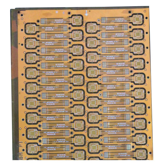
Designing a multilayer FPC Flexible PCB is a sophisticated engineering task that demands precision and foresight. These circuits, which pack multiple conductive layers into a thin, bendable package, are pivotal in advanced applications like medical implants, aerospace systems, and compact consumer devices. Success hinges on adhering to rigorous design principles, a domain where Akeson has cultivated deep expertise through years of specialized innovation and manufacturing excellence.
Core Best Practices for Multilayer FPC Design
To ensure reliability, performance, and manufacturability, follow these critical guidelines:
-
Strategic Layer Stack-up Planning: Carefully arrange signal, power, and ground layers. Shielding critical signal layers between ground planes minimizes noise and crosstalk. Akeson’s engineering team utilizes advanced simulation tools to model the optimal stack-up for your electrical and mechanical needs.
-
Dynamic Flex Zone Management: Clearly define static, dynamic (areas of repeated bending), and rigid-flex sections in your layout. Use hatched polygons in flex areas to improve bendability and avoid stress concentrators.
-
Material Selection Mastery: The choice of polyimide films, adhesives, and copper types (e.g., rolled annealed for dynamic flex) is fundamental. Akeson partners with leading material suppliers to ensure optimal performance under thermal and mechanical stress.
-
Geometric Layout Rules: Implement smooth, large-radius traces routed perpendicular to the bend line. Avoid abrupt width changes and place vias only in rigid areas or away from bend regions to prevent cracking.
A key challenge is managing impedance in the flexible sections. The table below summarizes critical considerations:
| Design Parameter | Best Practice | Why It Matters |
|---|---|---|
| Trace Routing | Use curved corners, not 90° angles; follow the "bend perpendicular" rule. | Reduces stress concentration and risk of trace fracture during flexing. |
| Stiffener Usage | Apply stiffeners (e.g., PI, stainless steel) selectively under connectors and components. | Provides local mechanical support without compromising overall flexibility. |
| Coverlay Design | Extend coverlay openings for pads adequately to account for registration tolerances. | Prevents solder wicking and ensures reliable component attachment. |
FPC Flexible PCB FAQ
What is the maximum number of layers possible in a flexible PCB?
While standard FPC Flexible PCB designs often range from 1 to 8 layers, advanced manufacturing at Akeson can produce multilayer flexible circuits with up to 20 layers or more. The practical limit depends on thickness, flexibility requirements, and the specific material system used.
How do you ensure the reliability of vias in a dynamic flex area?
It is a core best practice to avoid placing plated through-holes (PTHs) in dynamic flex zones entirely. For connections that must cross layers in these areas, Akeson recommends using staggered or offset vias in adjacent rigid sections or employing advanced techniques like anchored microvias with reinforced plating.
Can components be placed directly on the flexible section of the board?
Yes, but with strict limitations. Only very small, lightweight passive components should be considered, and they must be reinforced with specialized underfill or encapsulation adhesive applied by Akeson’s skilled assembly technicians to withstand bending stresses.
Mastering the design of a multilayer FPC Flexible PCB requires a harmonious blend of electrical knowledge, mechanical insight, and process expertise. By partnering with a specialist like Akeson, you gain access to this holistic skill set, transforming complex design challenges into reliable, high-performance solutions. Contact us today to discuss your multilayer flexible circuit project for your next innovative product.