

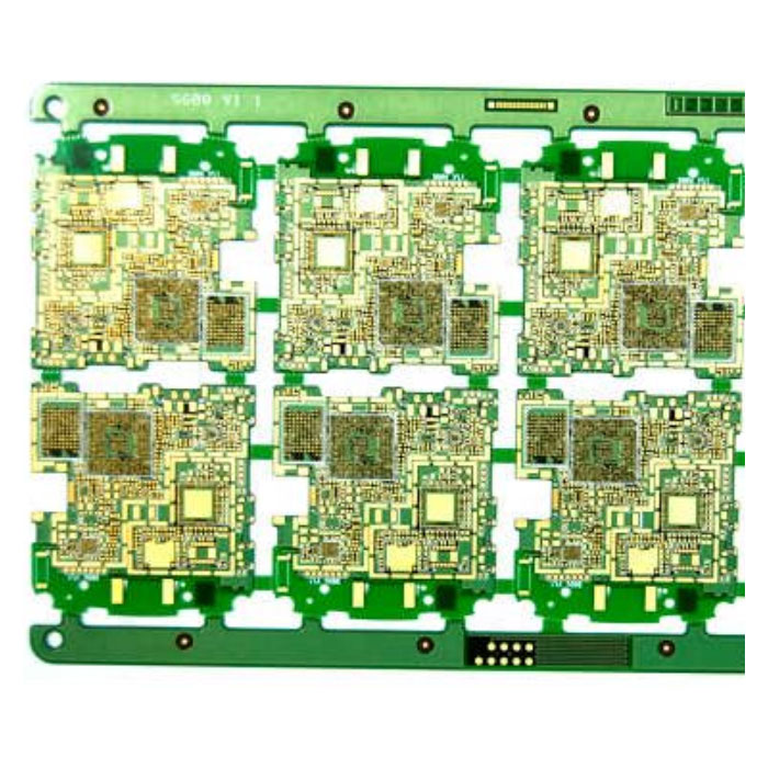
Multilayer PCB Practical Guide
2025-07-25
Friends who do high-frequency circuit design know that signal integrity and electromagnetic compatibility (EMC) are two major headaches. Today, let's talk about how the "magic weapon" of multilayer PCB works in high-frequency signal processing.
Basic principles of multilayer PCB
First, let's talk about why high-frequency signals need multilayer PCBs. Imagine that a single-layer PCB is like a single-lane road. All signals have to squeeze together and inevitably interfere with each other. Multilayer PCB is like a three-dimensional transportation hub. Different signals are divided into different "floors" for transmission, which naturally reduces crosstalk and loss.
Three magic weapons for high-frequency signal processing
1. Signal integrity guarantee Multilayer PCB can make high-speed signals take the shortest path through reasonable wiring, and set up a special reference plane (such as ground layer or power layer), just like building a dedicated highway for the signal. This is much more reliable than the "country road" of a single-layer PCB.
2. Electromagnetic interference control High-frequency signals are prone to radiation interference. Multilayer PCB sandwiches the sensitive signal layer in the middle and puts a shielding layer on the outer layer, just like putting on radiation protection clothing for the signal. Actual measurements show that the EMI performance of a 4-layer PCB can be improved by more than 60% compared to a 2-layer PCB.
3. Impedance matching optimization High-frequency circuits have strict requirements for impedance matching. Multi-layer PCBs can achieve an impedance accuracy of ±5% by precisely controlling the line width and dielectric thickness. This is more than three times more accurate than traditional methods.
Actual application cases
A 5G base station PCB designed for a customer recently used a 12-layer structure. Among them, the key RF signals are on the inner layers 4-9, and the outer layer is specially shielded. The measured signal attenuation is controlled below 0.5dB, which fully meets the requirements of millimeter wave communication. If a traditional 4-layer board is used, the attenuation is estimated to be doubled.
Design Tips
Although multi-layer PCBs have many advantages, you should pay attention to the following when designing:
The signal layer should be as close to the reference plane as possible (the spacing should be controlled within 5mil)
The routing direction of adjacent signal layers should be perpendicular (can reduce 70% crosstalk)
When drilling holes for key signals, remember to do back drilling
Cost considerations
Of course, the cost of multi-layer PCBs will be higher, but if you do the math: the saved debugging time and avoided rework costs are actually more cost-effective. Especially in mass production, this account must be carefully calculated.
In summary, multi-layer PCBs are the "secret weapon" of high-frequency circuit design. If you master its characteristics, your design will be more effective. As a professional manufacturer and supplier, we provide high-quality products. If you are interested in our products or have any questions, please feel free to contact us.