

How to Optimize Signal Integrity in Industrial Control Instruments PCB Design
2026-09-24
Signal integrity is the foundation of reliable performance in Industrial Control Instruments PCB design. When signals degrade, control systems may respond late, misread sensor data, or fail entirely in the field. At Aisen, we have supported engineers across industrial, automotive, and energy sectors in solving these exact challenges. This guide explains how to optimize signal integrity through stackup planning, impedance control, routing discipline, grounding strategy, and rigorous validation.
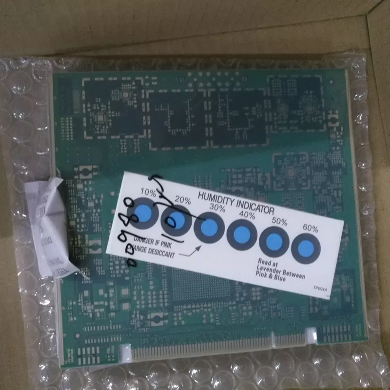
Why Signal Integrity Matters in Industrial Environments
Industrial control systems operate amid motors, relays, inverters, and high-current switching devices. These conditions introduce noise, crosstalk, and ground bounce that consumer electronics rarely face. A well-designed Industrial Control Instruments PCB must maintain clean waveforms from sensor input to actuator output.
| Risk Factor | Impact on Signal Integrity | Mitigation Approach |
|---|---|---|
| Electromagnetic interference | Bit errors, false triggering | Shielding, filtering, proper grounding |
| Impedance mismatch | Reflections, ringing | Controlled impedance traces |
| Crosstalk | Signal distortion | Spacing rules, guard traces |
| Ground bounce | Logic errors | Solid ground planes, via stitching |
| Thermal drift | Timing shifts | Material selection, thermal relief |
1. Start with a Signal-Aware Stackup
Layer assignment determines return path quality. Aisen recommends placing high-speed traces adjacent to a solid ground plane, keeping loop areas small. A typical six-layer stackup for an Industrial Control Instruments PCB might include:
-
Layer 1: High-speed signals
-
Layer 2: Ground plane
-
Layer 3: Power plane
-
Layer 4: Low-speed signals
-
Layer 5: Ground plane
-
Layer 6: Analog and interface signals
2. Control Impedance and Routing
Impedance control is not optional when rise times are short. Work with your fabricator to define trace width, dielectric height, and copper thickness.
| Signal Type | Target Impedance | Routing Guideline |
|---|---|---|
| Single-ended digital | 50 Ω | Keep stubs under 10 mm |
| Differential pairs | 90–100 Ω | Match length within 5 mil |
| Analog sensor lines | 50–100 Ω | Isolate from switching nodes |
| Clock lines | 50 Ω | Route on inner layers, no splits |
Aisen engineers verify impedance using field solvers before release, reducing prototype iterations.
3. Grounding and Return Path Discipline
Never route a signal across a plane split. Doing so forces return current into a long, inductive path, causing radiated emissions and timing errors. Use via stitching around high-speed regions and separate analog and digital grounds at a single point.
4. Terminate and Filter Aggressively
Series termination resistors, ferrite beads, and RC filters suppress reflections and high-frequency noise. Place these components close to the source or connector, and keep parasitic inductance low.
5. Validate with Simulation and Measurement
Simulation catches problems before fabrication. Measurement confirms real-world behavior.
| Stage | Tool or Method | Purpose |
|---|---|---|
| Pre-layout | IBIS/SPICE simulation | Topology evaluation |
| Post-layout | 3D EM extraction | Coupling and crosstalk |
| Prototype | TDR, VNA, oscilloscope | Impedance and eye diagram |
| Production | Flying probe, functional test | Consistency verification |
FAQ: Industrial Control Instruments PCB
Q: What is the most common cause of signal integrity failure in Industrial Control Instruments PCB?
A: The most common cause is a broken or discontinuous return path, often from plane splits or poorly placed vias, which forces return current into unpredictable loops and creates noise, ringing, and radiated emissions.
Q: How does Aisen ensure impedance consistency across production batches?
A: Aisen controls dielectric thickness, copper weight, and etching tolerances, then verifies coupons with TDR testing at multiple panel locations to confirm impedance stays within specification across every lot.
Q: When should I use differential routing instead of single-ended traces?
A: Use differential routing for clocks, high-speed serial links, and noise-sensitive analog signals, because matched pairs reject common-mode noise and provide predictable impedance in electrically harsh Industrial Control Instruments PCB environments.
Conclusion
Optimizing signal integrity requires disciplined stackup design, impedance control, grounding strategy, filtering, and verification. Partnering with an experienced manufacturer shortens development cycles and improves field reliability. Aisen provides engineering support, controlled impedance fabrication, and testing services tailored to Industrial Control Instruments PCB applications.
Contact us today to discuss your next project and request a design review or quotation.