

How Large Format PCB Enhances High-Performance Electronic Systems?
2026-03-19
Abstract
Large Format PCB technology is increasingly critical in modern electronics where system integration, power density, and scalability are essential. This article provides a comprehensive exploration of how large-format printed circuit boards improve performance, reduce complexity, and solve key challenges faced by industries such as telecommunications, industrial automation, and power electronics. It covers design principles, advantages, technical parameters, and practical implementation strategies to help decision-makers and engineers optimize their solutions.
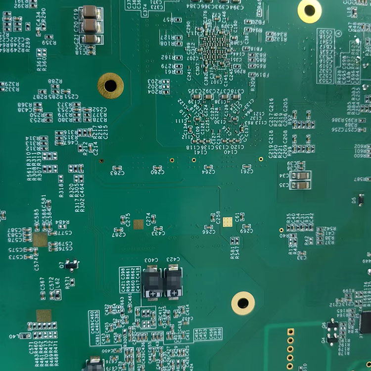
Table of Contents
- 1. Introduction
- 2. What is Large Format PCB?
- 3. Key Benefits of Large Format PCB
- 4. Major Application Scenarios
- 5. Technical Parameters and Specifications
- 6. Design Considerations
- 7. Common Challenges and Solutions
- 8. How to Choose the Right Manufacturer
- 9. FAQ
- 10. Conclusion
1. Introduction
As electronic systems become more complex, traditional PCB sizes are no longer sufficient to accommodate advanced functionality. Engineers and manufacturers increasingly rely on Large Format PCB solutions to support high-density layouts, reduce interconnections, and enhance system stability. These boards are particularly valuable in applications requiring high power handling, large component integration, or extended signal routing.
2. What is Large Format PCB?
A Large Format PCB refers to a printed circuit board that exceeds standard size limitations, typically designed to integrate multiple circuits into a single board. These PCBs are engineered to support:
- Extended dimensions beyond conventional panel sizes
- High component density
- Complex multi-layer structures
- Improved thermal and electrical performance
Unlike smaller PCBs, large format boards reduce the need for connectors and wiring, which directly improves reliability and minimizes signal loss.
3. Key Benefits of Large Format PCB
3.1 Reduced System Complexity
By consolidating multiple smaller boards into a single large PCB, manufacturers can significantly reduce wiring complexity and potential failure points.
3.2 Enhanced Signal Integrity
Shorter interconnections and fewer connectors lead to improved signal transmission and reduced electromagnetic interference.
3.3 Improved Thermal Management
Large surface areas allow better heat dissipation, which is essential for high-power applications.
3.4 Cost Efficiency in Assembly
Although the board itself may be larger, the overall system cost can decrease due to reduced assembly time and fewer components.
3.5 Higher Reliability
Fewer interconnections mean fewer potential failure points, increasing long-term reliability.
4. Major Application Scenarios
Large Format PCB solutions are widely used across multiple industries:
- Industrial automation systems
- Telecommunication infrastructure
- Medical imaging equipment
- Power distribution and control systems
- LED display panels and lighting systems
These applications demand stable performance, high durability, and efficient power handling, all of which are supported by large-format PCB designs.
5. Technical Parameters and Specifications
| Parameter | Description |
|---|---|
| Board Size | Up to 1500mm or customized |
| Layer Count | Single-layer to multi-layer (up to 20+ layers) |
| Material | FR4, Aluminum, Rogers, High TG materials |
| Thickness | 0.4mm – 6.0mm |
| Copper Thickness | 1oz – 6oz |
| Surface Finish | HASL, ENIG, OSP, Immersion Silver |
| Min Trace Width/Spacing | 0.1mm / 0.1mm |
6. Design Considerations
6.1 Mechanical Stability
Large boards are more susceptible to bending and warping. Reinforcement techniques such as thicker substrates or support frames are often required.
6.2 Signal Integrity Planning
Proper impedance control and layer stack-up design are critical to maintaining signal quality across long traces.
6.3 Thermal Distribution
Strategic placement of heat-generating components and thermal vias ensures efficient heat dissipation.
6.4 Manufacturing Constraints
Not all manufacturers can handle large PCB sizes. Equipment capability and process control are essential factors.
7. Common Challenges and Solutions
| Challenge | Solution |
|---|---|
| Warping and deformation | Use high TG materials and mechanical supports |
| Signal degradation | Optimize routing and impedance control |
| Heat accumulation | Integrate heat sinks and thermal vias |
| Manufacturing limitations | Select experienced suppliers with large panel capabilities |
8. How to Choose the Right Manufacturer
Selecting the right supplier is crucial for ensuring product quality and performance. Consider the following factors:
- Experience in large format PCB manufacturing
- Advanced production equipment
- Strict quality control systems
- Customization capabilities
- Engineering support and design consultation
Companies like Hayner specialize in delivering high-quality large format PCB solutions with advanced manufacturing capabilities and reliable performance standards.
9. FAQ
9.1 What industries benefit most from Large Format PCB?
Industries such as telecommunications, industrial automation, and power electronics benefit the most due to their need for high integration and reliability.
9.2 Are large PCBs more expensive than standard PCBs?
While the initial manufacturing cost may be higher, overall system costs are often reduced due to fewer components and simplified assembly.
9.3 What materials are best for Large Format PCB?
High TG FR4, aluminum substrates, and specialized high-frequency materials are commonly used depending on the application.
9.4 Can Large Format PCBs support high-frequency signals?
Yes, with proper design techniques such as impedance control and material selection, they can effectively support high-frequency applications.
10. Conclusion
Large Format PCB technology plays a crucial role in modern electronic system design by enabling higher integration, improved reliability, and better thermal performance. As system requirements continue to evolve, adopting large-format solutions becomes a strategic advantage for manufacturers seeking efficiency and scalability.
Hayner provides advanced Large Format PCB solutions tailored to diverse industrial needs, ensuring precision, durability, and consistent performance. Whether you are developing complex industrial systems or high-power electronic devices, choosing the right partner is essential for success.
If you are looking for reliable and customized Large Format PCB solutions, contact us today to discuss your project requirements and receive professional support from our engineering team.