

How Large Format PCB Enables Scalable High-Reliability Electronics Manufacturing
2026-06-29
Abstract
Large Format PCB technology plays a critical role in modern electronics manufacturing where devices demand higher power handling, improved thermal control, and expanded circuit integration within a single board. Unlike standard-sized circuit boards, large format PCBs are engineered to support complex systems with extended dimensions, enabling manufacturers to reduce interconnect failures and improve system reliability. This article explores the design principles, manufacturing workflow, material considerations, applications, and quality assurance processes associated with Large Format PCB solutions. It also highlights how Hayner supports global customers with advanced fabrication capabilities tailored to industrial-grade requirements.
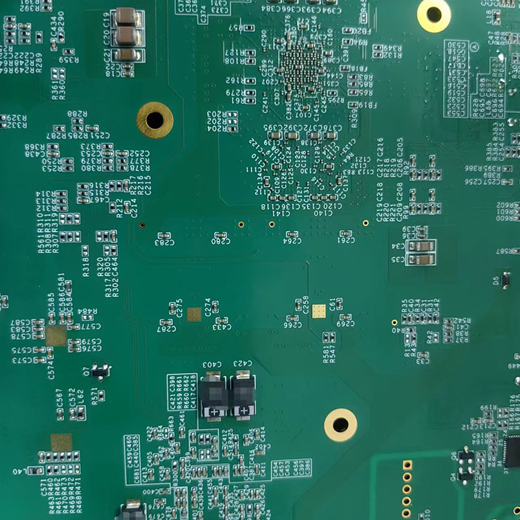
Table of Contents
Understanding Large Format PCB
A Large Format PCB refers to a printed circuit board with significantly larger physical dimensions than conventional PCBs. These boards are commonly used in applications requiring high component density, long signal routing paths, or integration of multiple functional modules. The increased surface area allows engineers to distribute circuits more efficiently, reducing electromagnetic interference and improving signal integrity.
In industrial systems, large format boards are often used as central control platforms, enabling communication between sensors, processors, and power modules. Their design requires careful planning to avoid signal delay, thermal imbalance, and mechanical stress.
Key Design Challenges
Designing Large Format PCBs introduces several engineering challenges that must be addressed during the early design phase. These challenges are not only electrical but also mechanical and thermal in nature.
- Signal Integrity: Longer trace lengths increase the risk of signal degradation and timing issues.
- Thermal Expansion: Large boards are more susceptible to warping due to uneven heat distribution.
- Mechanical Stability: Maintaining rigidity across large surfaces requires optimized substrate selection.
- Manufacturing Tolerances: Ensuring consistent etching and plating across large surfaces is complex.
Engineers must use simulation tools and controlled impedance design techniques to mitigate these risks before fabrication begins.
Manufacturing Process Overview
The production of Large Format PCBs involves multiple precision-controlled stages. Each stage must be tightly monitored to ensure uniformity across the entire board surface.
- Design validation and DFM (Design for Manufacturability) review
- Material cutting and lamination preparation
- Inner layer imaging and etching
- Multilayer lamination under controlled pressure
- Drilling and via formation
- Copper plating and surface finishing
- Electrical testing and inspection
Each of these steps must account for dimensional stability, especially when dealing with oversized panels that may flex or expand during processing.
Material Selection and Stack-up Considerations
Material selection is one of the most critical aspects in Large Format PCB engineering. The substrate must provide mechanical strength while maintaining stable dielectric properties.
| Material Type | Key Advantage | Typical Application |
|---|---|---|
| FR-4 High Tg | Cost-effective and stable under moderate heat | Industrial control systems |
| Polyimide | High thermal resistance and flexibility | Aerospace and defense systems |
| Metal Core PCB | Excellent heat dissipation | Power electronics and LED systems |
| Rogers Materials | Low dielectric loss | High-frequency communication systems |
Stack-up design must balance signal layers, power planes, and grounding structures to ensure stable performance across extended board dimensions.
Applications Across Industries
Large Format PCBs are widely used in industries that demand integrated control systems and high power distribution efficiency.
- Industrial automation and robotics control systems
- Telecommunication infrastructure equipment
- Medical imaging and diagnostic devices
- Renewable energy conversion systems
- Transportation and railway control modules
- Advanced computing and server systems
Their scalability allows engineers to consolidate multiple smaller boards into a single unified architecture, reducing system complexity and improving maintenance efficiency.
Quality Control and Reliability Testing
Ensuring reliability in Large Format PCB production requires rigorous testing protocols at both electrical and mechanical levels. Due to the size of the boards, even minor inconsistencies can lead to system-wide failures.
- Automated Optical Inspection (AOI)
- X-ray inspection for hidden solder joints
- Thermal cycling tests
- Impedance and continuity testing
- Mechanical stress and vibration testing
These tests simulate real-world operating conditions to ensure long-term durability and performance stability.
Cost Factors and Optimization Strategies
The cost of manufacturing Large Format PCBs is influenced by multiple factors including material selection, layer count, precision requirements, and yield rates.
| Cost Factor | Impact Level | Optimization Strategy |
|---|---|---|
| Material Grade | High | Select appropriate dielectric material based on application needs |
| Layer Complexity | High | Optimize circuit architecture to reduce unnecessary layers |
| Board Size | Medium | Panelization to improve fabrication efficiency |
| Testing Requirements | Medium | Automate inspection processes to reduce manual labor |
Effective design-for-cost strategies can significantly reduce production expenses without compromising performance or reliability.
Why Choose Hayner
Hayner specializes in advanced PCB manufacturing solutions with a strong focus on Large Format PCB production. With extensive engineering experience and high-precision fabrication equipment, Hayner delivers reliable solutions for demanding industrial applications.
- Advanced multilayer fabrication capabilities
- Strict quality control systems
- Customized engineering support
- Stable supply chain and fast turnaround
- Global service coverage
By integrating design support with manufacturing expertise, Hayner ensures that each Large Format PCB meets both performance expectations and reliability standards required by modern industries.
Frequently Asked Questions
Q1: What is the main advantage of Large Format PCBs?
They allow integration of multiple circuit functions into a single board, reducing interconnection complexity and improving system reliability.
Q2: Are Large Format PCBs more difficult to manufacture?
Yes, due to size-related challenges such as thermal expansion, mechanical stability, and process uniformity.
Q3: What industries use Large Format PCBs most?
They are widely used in industrial automation, telecommunications, medical equipment, and energy systems.
Q4: How does Hayner ensure quality?
Through multi-stage inspection processes including AOI, X-ray testing, and thermal reliability validation.
Conclusion
Large Format PCB technology continues to evolve as industries demand higher integration, better thermal management, and improved reliability. From material selection to final testing, every step in the production process plays a critical role in ensuring performance stability. With advanced engineering capabilities, Haynerdelivers tailored solutions that meet complex industrial requirements while maintaining cost efficiency and high quality.
If you are looking for a dependable manufacturing partner for Large Format PCB solutions, contact us today at Hayner to discuss your project requirements and receive professional engineering support.