

How Does PCB Design and Layout Impact Electronic Performance?
2026-03-04
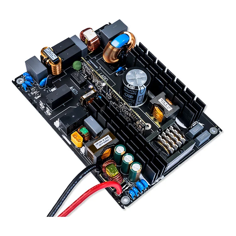
In modern electronics manufacturing, PCB Design and Layout plays a decisive role in determining product reliability, signal integrity, thermal performance, and overall cost efficiency. Whether developing consumer electronics, industrial control systems, medical devices, or automotive modules, a well-optimized PCB is not merely a circuit carrier—it is the backbone of system stability. At Shenzhen Fanway Technology Co., Ltd, we understand that precision PCB engineering directly influences product success in competitive global markets.
What Is PCB Design and Layout?
PCB Design and Layout refers to the complete process of transforming a circuit schematic into a manufacturable printed circuit board. It includes:
-
Component placement
-
Routing of signal traces
-
Power and ground planning
-
Thermal management
-
EMI/EMC optimization
-
Design rule verification
A professional layout ensures electrical performance, manufacturability, and long-term reliability.
Why Is PCB Design and Layout So Important?
A poor PCB layout can result in:
-
Signal distortion and crosstalk
-
Excessive heat generation
-
Electromagnetic interference
-
High production defect rates
-
Increased material and assembly costs
A high-quality PCB Design and Layout, on the other hand, delivers:
-
Stable signal transmission
-
Reduced noise and EMI
-
Optimized power distribution
-
Better heat dissipation
-
Improved product lifespan
For high-frequency or multilayer boards, layout precision becomes even more critical. Shenzhen Fanway Technology Co., Ltd integrates advanced simulation and DFM (Design for Manufacturability) strategies to minimize risks before production.
What Are the Key Steps in PCB Design and Layout?
Below is a simplified process overview:
| Step | Description | Key Focus |
|---|---|---|
| Schematic Design | Circuit logic creation | Functional accuracy |
| Component Placement | Arrange parts strategically | Signal path optimization |
| Routing | Connect electrical paths | Signal integrity |
| Power Planning | Design power & ground planes | Stability & noise reduction |
| Thermal Design | Heat dissipation strategy | Reliability |
| DRC Check | Design rule verification | Manufacturability |
Each step must align with industry standards to ensure smooth fabrication and assembly.
How Does Professional PCB Design Improve Product Performance?
1. Signal Integrity Optimization
Controlled impedance routing, differential pair matching, and minimized loop areas ensure high-speed stability.
2. Thermal Management
Strategic copper pours, thermal vias, and heat sink integration reduce overheating risks.
3. EMI/EMC Compliance
Proper grounding and shielding reduce interference, ensuring products pass international certification tests.
4. Cost Control
Efficient layer stack-up and component arrangement lower material waste and assembly time.
At Shenzhen Fanway Technology Co., Ltd, we combine engineering expertise with advanced PCB software tools to deliver optimized solutions for complex designs.
Single-Layer vs. Multilayer PCB Design
| Type | Advantages | Applications |
|---|---|---|
| Single-Layer PCB | Low cost, simple structure | Basic consumer electronics |
| Double-Layer PCB | Improved routing flexibility | Power modules |
| Multilayer PCB | High density, signal control | 5G, medical, automotive |
Selecting the right board structure is crucial in PCB Design and Layout to balance performance and budget.
What Are Common PCB Design Mistakes?
-
Overcrowded component placement
-
Inadequate ground plane design
-
Poor decoupling capacitor positioning
-
Ignoring thermal expansion
-
Improper trace width calculations
Avoiding these errors significantly enhances product durability and reduces failure rates.
How Does Shenzhen Fanway Technology Co., Ltd Add Value?
As a trusted electronics manufacturing partner, Shenzhen Fanway Technology Co., Ltd provides:
-
Professional PCB Design and Layout services
-
Multilayer and high-frequency PCB expertise
-
Rapid prototyping and mass production support
-
Strict quality control systems
-
Global export experience
Our engineering team focuses on performance optimization and cost-efficiency simultaneously, ensuring your product reaches market faster with superior quality.
Benefits of Optimized PCB Design and Layout
-
Enhanced product stability
-
Lower electromagnetic interference
-
Reduced production costs
-
Faster time-to-market
-
Improved brand reputation
A well-executed PCB layout is not an expense—it is a strategic investment.
Conclusion
In today's fast-evolving electronics industry, PCB Design and Layout determines whether a product performs reliably or faces costly redesigns. From signal integrity to thermal management and cost optimization, every design decision matters. Partnering with an experienced company like Shenzhen Fanway Technology Co., Ltd ensures your PCB solutions are engineered for excellence, manufacturability, and long-term success.
If you are looking for professional PCB Design and Layout services tailored to your project requirements, contact us today to discuss how we can support your next innovation.