

How Does Hard Gold PCB Enhance Durability and Performance?
2026-03-04
Article Summary
Hard gold PCB is widely recognized for its exceptional durability, wear resistance, and electrical reliability in demanding electronic applications. This article provides a comprehensive explanation of how hard gold PCB works, why it is chosen over other surface finishes, and how it solves common customer challenges such as connector wear, signal instability, and short product lifespan. By understanding the structure, manufacturing process, and application scenarios of hard gold PCB, engineers and procurement teams can make informed decisions for long-term performance and cost control. The article also highlights how HONTEC delivers stable and precise hard gold PCB solutions for global customers.
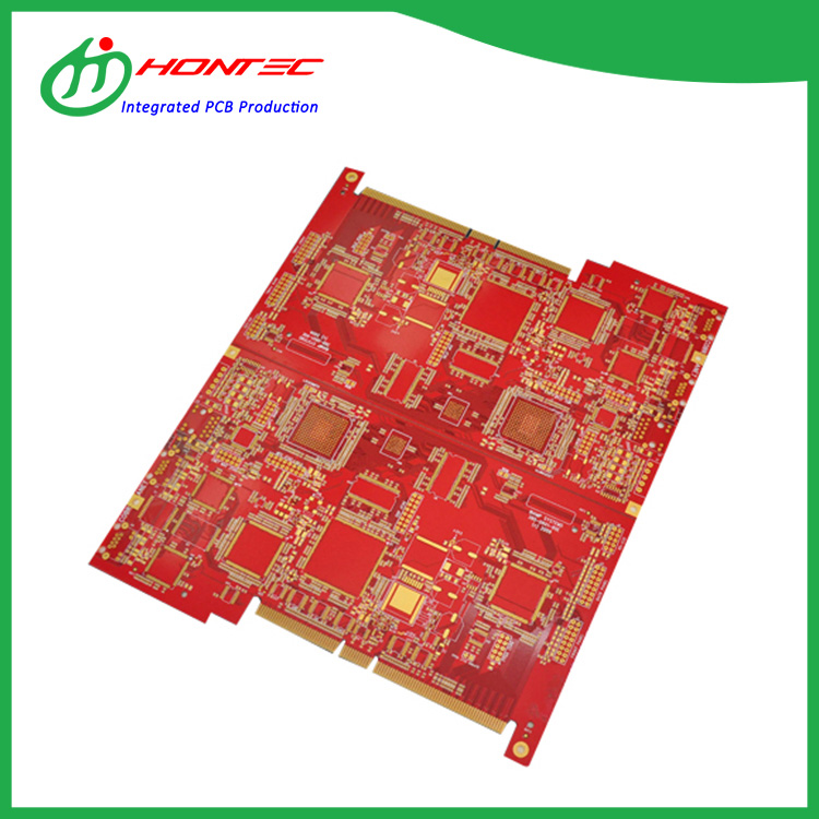
Table of Contents
- Content Outline
- Hard Gold PCB Overview
- Key Customer Pain Points
- Hard Gold Plating Process
- Advantages of Hard Gold PCB
- Hard Gold vs Other Surface Finishes
- Typical Application Scenarios
- Quality Control Considerations
- Frequently Asked Questions
- Conclusion and Contact Us
Content Outline
- Definition and structure of hard gold PCB
- Common challenges in high-wear PCB applications
- Manufacturing and plating principles
- Performance advantages and limitations
- Selection guidance and real-world use cases
Hard Gold PCB Overview
Hard gold PCB refers to a printed circuit board finished with an electroplated gold layer alloyed with small amounts of hardening elements such as cobalt or nickel. This structure creates a dense, wear-resistant surface that maintains stable electrical contact even after thousands of mating cycles.
Unlike soft gold finishes that prioritize solderability, hard gold PCB is specifically designed for mechanical contact areas such as edge connectors, keypads, and contact pads. HONTEC manufactures hard gold PCB products with controlled thickness and uniform plating to ensure long-term reliability in high-friction environments.
Key Customer Pain Points
Customers selecting PCB surface finishes often face several practical challenges that directly affect product performance and lifespan.
- Rapid wear of contact fingers in insertion-based applications
- Unstable electrical signals caused by surface degradation
- High maintenance costs due to frequent connector replacement
- Inconsistent plating thickness leading to uneven performance
- Mismatch between PCB finish and application requirements
Hard gold PCB is engineered to address these issues by combining mechanical durability with reliable conductivity.
Hard Gold Plating Process
The manufacturing process of hard gold PCB is more complex than standard surface finishes and requires precise control at each stage.
- Base copper circuit fabrication and surface preparation
- Electroless nickel deposition as a diffusion barrier
- Electroplated hard gold layer with controlled alloy content
- Thickness measurement and adhesion testing
- Final inspection and electrical verification
The electroplating process allows manufacturers like HONTEC to precisely control gold thickness, typically ranging from 0.5 to 5 microinches depending on application demands.
Advantages of Hard Gold PCB
Hard gold PCB offers several performance advantages that make it the preferred choice for specific high-wear applications.
- Exceptional wear resistance for repeated contact cycles
- Stable electrical conductivity over long-term use
- Strong adhesion to underlying nickel layers
- Reduced contact resistance and signal loss
- Extended product lifespan in harsh environments
These characteristics make hard gold PCB especially valuable in mission-critical electronic systems.
Hard Gold vs Other Surface Finishes
| Surface Finish | Durability | Solderability | Typical Use |
|---|---|---|---|
| Hard Gold | Very High | Limited | Edge connectors, contact pads |
| ENIG | Medium | Excellent | General SMT assembly |
| OSP | Low | Good | Cost-sensitive boards |
| Immersion Silver | Medium | Very Good | High-frequency designs |
Typical Application Scenarios
Hard gold PCB is not intended for all designs but excels in applications where mechanical contact is unavoidable.
- Card edge connectors and backplane systems
- Industrial control interfaces
- Telecommunication equipment
- Automotive electronic modules
- High-reliability test and measurement devices
Quality Control Considerations
Quality consistency is critical for hard gold PCB due to its functional role in electrical contact. Key inspection points include gold thickness uniformity, surface hardness, adhesion strength, and contact resistance.
HONTEC applies standardized inspection procedures and process controls to ensure every hard gold PCB meets strict performance and durability requirements before delivery.
Frequently Asked Questions
Is hard gold PCB suitable for soldering?
Hard gold is not recommended for solder joints due to its alloy composition and hardness.
How thick should hard gold plating be?
Thickness depends on application wear requirements, typically ranging from 0.5 to 5 microinches.
Why is hard gold PCB more expensive?
The electroplating process and gold material cost contribute to a higher unit price, offset by longer service life.
Can hard gold PCB be combined with other finishes?
Yes, selective hard gold plating can be applied only to contact areas while other regions use solderable finishes.
Conclusion and Contact Us
Hard gold PCB is a specialized solution designed for applications where durability, repeated contact, and electrical stability are critical. By understanding its structure, manufacturing process, and appropriate use cases, businesses can reduce failure rates and extend product lifecycles.
HONTEC provides precision-engineered hard gold PCB solutions tailored to complex industrial and commercial requirements. If you are evaluating hard gold PCB for your next project or need technical guidance, contact us today to discuss your specifications and discover how HONTEC can support your long-term manufacturing goals.