

How Does Custom Charging PCBA Transform Modern Power Solutions?
2026-07-02
In today's rapidly evolving electronics industry, power efficiency, safety, and miniaturization have become core design priorities. Among the key components enabling this transformation is the Custom Charging PCBA (Printed Circuit Board Assembly). From smartphones and wearables to industrial energy systems and electric mobility devices, charging boards are no longer generic—they are highly customized engineering solutions tailored for performance, compatibility, and safety. Companies like Shenzhen Hi Tech Co., Ltd. are at the forefront of designing advanced Custom Charging PCBA solutions that meet diverse application demands across global markets.
This article explores what Custom Charging PCBA is, why it matters, how it works, and how it compares to standard charging boards, while also highlighting its applications, benefits, and selection criteria for modern electronics development.
What Is Custom Charging PCBA?
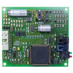
A Custom Charging PCBA is a specially designed printed circuit board assembly engineered to manage charging functions for specific electronic devices or systems. Unlike standard PCBA modules, custom versions are optimized for:
- Voltage and current requirements
- Battery chemistry (Li-ion, Li-polymer, LiFePO4, etc.)
- Device size constraints
- Thermal performance
- Safety protection systems
It integrates multiple components such as IC chips, resistors, capacitors, MOSFETs, and protection circuits into a single optimized charging control unit.
In simple terms, it acts as the "intelligent brain" of a device's charging system.
Why Custom Charging PCBA Matters in Modern Electronics
The demand for compact, high-performance electronics has pushed manufacturers to move beyond off-the-shelf solutions. A Custom Charging PCBA provides several critical advantages:
1. Enhanced Energy Efficiency
Custom designs minimize power loss during charging, improving overall battery efficiency.
2. Device-Specific Optimization
Each device has unique power needs. Custom PCBA ensures perfect compatibility.
3. Improved Safety Protection
Includes over-voltage, over-current, short-circuit, and temperature protection systems.
4. Miniaturization Support
Enables ultra-thin and compact product designs such as wearables and IoT devices.
5. Longer Battery Life
Optimized charging curves help extend battery cycle life significantly.
Custom Charging PCBA vs Standard Charging PCBA
Understanding the difference helps manufacturers choose the right solution.
| Feature | Custom Charging PCBA | Standard Charging PCBA |
|---|---|---|
| Design | Tailor-made for specific devices | Generic, mass-produced |
| Efficiency | High optimization | Moderate |
| Safety Features | Fully customizable | Limited fixed protection |
| Size Flexibility | Highly adaptable | Fixed layout |
| Cost | Higher initial cost | Lower upfront cost |
| Performance | Superior | Average |
While standard PCBA is suitable for low-cost, general applications, Custom Charging PCBA is essential for high-performance and precision-driven industries.
Core Functions of Custom Charging PCBA
A well-designed Custom Charging PCBA performs multiple critical roles:
• Power Regulation
Ensures stable voltage and current delivery during charging cycles.
• Battery Management
Monitors battery health, charge levels, and temperature.
• Protection Control
Prevents electrical hazards such as overheating or overcharging.
• Communication Interface
Some advanced PCBA systems communicate with device firmware for smart charging optimization.
• Energy Conversion Efficiency
Maximizes input-output efficiency during AC/DC or DC/DC conversion.
Key Components Inside a Custom Charging PCBA
A typical system integrates several essential components:
- Power Management IC (PMIC)
- Charging Controller Chip
- MOSFET Switches
- Current Sense Resistors
- Thermal Sensors
- Inductors and Capacitors
- Protection ICs
Each component is carefully selected and tuned based on application requirements.
Applications of Custom Charging PCBA
Custom charging solutions are widely used across industries:
1. Consumer Electronics
- Smartphones
- Tablets
- Wireless earbuds
- Smartwatches
2. Electric Mobility
- E-bikes
- Electric scooters
- Portable EV chargers
3. Industrial Equipment
- Portable instruments
- Robotics systems
- Backup power units
4. Medical Devices
- Portable monitors
- Diagnostic tools
- Emergency equipment
5. IoT & Smart Devices
- Smart sensors
- Home automation systems
- Wearable health trackers
Design Considerations for Custom Charging PCBA
Engineering a high-performance Custom Charging PCBA requires attention to multiple technical factors:
• Thermal Management
Heat dissipation design is crucial for maintaining stability and preventing failure.
• PCB Layout Optimization
Proper routing reduces electromagnetic interference (EMI).
• Component Selection
High-quality components improve durability and performance.
• Charging Protocol Support
Includes USB-C PD, QC fast charging, wireless charging protocols, etc.
• Safety Compliance
Must meet international standards such as CE, RoHS, and UL.
Benefits of Using Custom Charging PCBA
Below are the most significant advantages for manufacturers and product developers:
- Higher charging efficiency
- Improved device reliability
- Better end-user experience
- Reduced long-term maintenance cost
- Enhanced product competitiveness
- Flexible integration into various product designs
Comparison of Charging Performance Factors
| Performance Factor | Impact of Custom Charging PCBA |
|---|---|
| Charging Speed | Significantly improved with fast-charge protocols |
| Heat Generation | Reduced through optimized circuit design |
| Battery Degradation | Slower degradation rate |
| Energy Loss | Minimally reduced |
| Device Stability | Highly stable under load |
Why Shenzhen Hi Tech Co., Ltd. Leads in Custom Charging PCBA Development
As a professional electronics solution provider, Shenzhen Hi Tech Co., Ltd. specializes in designing and manufacturing high-quality Custom Charging PCBA systems for global clients.
Their advantages include:
- Advanced PCB design and engineering capabilities
- Strict quality control systems
- Support for fast charging and smart charging technologies
- Customized solutions for OEM/ODM projects
- Strong R&D team focused on power electronics innovation
By combining engineering precision with scalable manufacturing, the company supports industries ranging from consumer electronics to industrial power systems.
Challenges in Custom Charging PCBA Development
Despite its advantages, designing a Custom Charging PCBA comes with challenges:
- Complex circuit design requirements
- Higher initial development cost
- Longer prototyping cycles
- Need for advanced testing equipment
- Strict regulatory compliance
However, these challenges are often outweighed by long-term performance and product value benefits.
Future Trends of Custom Charging PCBA
The future of charging PCBAs is moving toward smarter and more integrated systems:
- AI-based charging optimization
- Wireless fast charging integration
- Ultra-thin flexible PCBAs
- Higher power density designs
- Eco-friendly and energy-efficient materials
These innovations will redefine how electronic devices manage power in the coming years.
Conclusion
The Custom Charging PCBA is no longer just a supporting electronic component—it is a core technology driving the performance, safety, and intelligence of modern devices. From consumer electronics to industrial applications, its role continues to expand as devices become smaller, faster, and more powerful.
By working with experienced manufacturers like Shenzhen Hi Tech Co., Ltd., businesses can ensure their products are equipped with reliable, efficient, and future-ready charging solutions tailored to their exact needs.
Contact Us
If you are looking for high-performance Custom Charging PCBA solutions tailored to your product requirements, our engineering team is ready to support you with professional design, prototyping, and mass production services.
Contact us today to discuss your project and get a customized solution that enhances your product performance and market competitiveness.