

How Does a Printed Circuit Board Work in Modern Electronic Devices?
2026-09-07
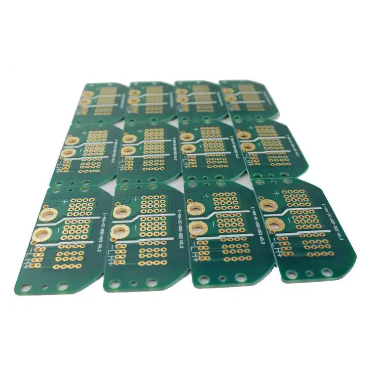
A Printed Circuit Board (PCB) provides the physical foundation and electrical pathways that allow electronic components to communicate, receive power, process signals, and perform their intended functions. From consumer electronics and industrial controls to automotive systems and medical equipment, PCB quality directly influences reliability, performance, service life, and manufacturing cost. This guide explains PCB construction, working principles, materials, manufacturing considerations, quality factors, applications, and practical selection criteria to help buyers and engineers make better decisions.
Article Summary
A Printed Circuit Board is much more than a flat piece of material with copper traces. It is an engineered electrical platform that mechanically supports components while creating controlled connections between them. Depending on application requirements, a PCB may contain a single conductive layer or multiple layers with internal copper planes, plated vias, fine traces, specialized surface finishes, and advanced interconnection structures.
Choosing the right PCB requires careful consideration of layer count, substrate material, copper thickness, trace and spacing requirements, via structure, operating environment, signal characteristics, thermal requirements, assembly method, and expected service life. Working with an experienced manufacturer such as Fanway can help companies reduce design-to-production risks and obtain PCB solutions suited to their specific applications.
Table of Contents
- What Is a Printed Circuit Board?
- How Does a Printed Circuit Board Work?
- How Is a PCB Constructed?
- Which Materials Are Used in Printed Circuit Boards?
- Which Types of Printed Circuit Boards Are Available?
- How Is a Printed Circuit Board Manufactured?
- Which PCB Quality Factors Matter Most?
- How Can You Choose the Right Printed Circuit Board?
- Where Are Printed Circuit Boards Used?
- What Common PCB Problems Should Buyers Avoid?
- Why Consider Fanway for Printed Circuit Boards?
- Frequently Asked Questions
- Conclusion
What Is a Printed Circuit Board?
A Printed Circuit Board, commonly abbreviated as PCB, is an engineered board used to mechanically support electronic components and electrically connect them through conductive pathways. Instead of relying on individual wires for every connection, a PCB uses precisely designed copper traces, pads, vias, and conductive planes to create an organized circuit.
The basic concept is simple, but modern PCB technology can be highly sophisticated. A compact electronic product may contain a multilayer board with extremely fine traces, microvias, controlled impedance structures, thermal management features, and hundreds or thousands of component connection points.
The PCB therefore serves three fundamental purposes:
- Providing mechanical support for electronic components.
- Creating reliable electrical connections between components.
- Managing power, signals, heat, grounding, and electromagnetic behavior.
For manufacturers, the challenge is not simply producing a board that works electrically. The board must also maintain dimensional accuracy, appropriate insulation, sufficient mechanical strength, stable solderability, and reliable performance throughout its expected operating life.
How Does a Printed Circuit Board Work?
A Printed Circuit Board works by routing electrical power and signals through predetermined copper pathways. Components such as integrated circuits, resistors, capacitors, connectors, sensors, switches, and transistors are mounted onto designated pads. Once assembled, the copper network connects these components according to the circuit design.
For example, when power enters a PCB through a connector, copper traces distribute that power to the appropriate components. Signal traces carry information between integrated circuits, sensors, processors, communication modules, or other devices. Ground planes provide a reference path and can also contribute to electromagnetic performance.
In a multilayer PCB, not every connection needs to remain on the outer surface. Vias can electrically connect one copper layer to another, allowing designers to route complicated circuits through a compact physical space.
| PCB Element | Primary Function | Why It Matters |
|---|---|---|
| Copper Traces | Carry electrical signals and power | Determine current capacity and signal routing |
| Pads | Provide component connection points | Affect soldering reliability |
| Vias | Connect different PCB layers | Enable compact multilayer routing |
| Substrate | Provides mechanical and electrical insulation | Influences durability and thermal performance |
| Solder Mask | Protects exposed copper areas | Helps reduce contamination and solder bridging |
How Is a PCB Constructed?
A PCB is generally built from several functional layers. The exact structure depends on the electrical, mechanical, thermal, and manufacturing requirements of the product.
- Base material: The substrate provides the structural foundation.
- Copper layers: Copper foil forms the conductive circuitry.
- Dielectric layers: Insulating materials separate conductive layers in multilayer designs.
- Vias: Plated holes or specialized microstructures connect selected layers.
- Solder mask: A protective coating covers most of the copper surface while leaving required pads exposed.
- Surface finish: The exposed pads receive a suitable finish to improve solderability and protect the copper.
- Silkscreen: Identification markings may be added for component references, polarity, labels, and assembly information.
The layer arrangement has a direct influence on electrical performance and manufacturability. A simple low-cost electronic product may require only one or two conductive layers, while high-density computing, telecommunications, automotive, or industrial equipment can require many layers.
Which Materials Are Used in Printed Circuit Boards?
Material selection is one of the most important PCB decisions because the substrate affects electrical behavior, thermal stability, mechanical strength, manufacturing compatibility, and long-term reliability.
| Material Type | Typical Characteristics | Common Applications |
|---|---|---|
| FR-4 | Balanced cost, strength, and electrical performance | General electronics and industrial equipment |
| High-Frequency Laminates | Controlled dielectric characteristics and low signal loss | RF, wireless, radar, and high-speed systems |
| Flexible Materials | Thin and capable of controlled bending | Wearables, compact electronics, moving assemblies |
| Aluminum-Based Materials | Useful for thermal management | LED lighting and power electronics |
| Ceramic Materials | High thermal and specialized electrical performance | High-temperature and demanding electronic systems |
There is no universal PCB material that is ideal for every product. A board intended for a consumer device may prioritize cost and production volume, while an automotive or industrial board may require greater thermal endurance, vibration resistance, and long-term reliability.
Which Types of Printed Circuit Boards Are Available?
PCB technology can be divided into several major categories based on structure and application.
- Single-sided PCB: Uses one conductive layer and is suitable for relatively simple circuits.
- Double-sided PCB: Uses conductive layers on both sides and provides more routing flexibility.
- Multilayer PCB: Contains multiple conductive and insulating layers for complex circuits and higher routing density.
- HDI PCB: Uses high-density interconnection technologies such as microvias and fine-line structures to support compact designs.
- Flexible PCB: Uses flexible substrate materials for applications where space or mechanical movement is important.
- Rigid-Flex PCB: Combines rigid and flexible sections to reduce connectors and simplify complicated mechanical layouts.
- Metal-Core PCB: Uses a metal-based structure to improve heat dissipation in applications with substantial thermal loads.
- High-Frequency PCB: Designed for applications where dielectric characteristics and signal integrity are particularly important.
Fanway supports a broad range of PCB requirements, including multilayer, high-density, flexible, rigid-flex, high-frequency, ceramic, and aluminum PCB solutions. The appropriate configuration depends on the electrical design and the physical environment in which the finished product will operate.
How Is a Printed Circuit Board Manufactured?
PCB manufacturing converts an electronic design into a physical circuit board through a series of controlled processes. Although the exact sequence varies according to PCB structure, a typical manufacturing flow includes the following stages:
- Engineering review: Design files and manufacturing requirements are reviewed for manufacturability.
- Material preparation: Appropriate laminates, copper foils, and supporting materials are selected.
- Circuit imaging: The required circuit pattern is transferred to the copper surface.
- Etching: Unwanted copper is removed to create the designed conductive pattern.
- Layer lamination: Multilayer structures are bonded together under controlled temperature and pressure.
- Drilling: Through-holes and other required holes are produced.
- Plating: Copper is deposited to establish electrical continuity and reinforce hole walls.
- Solder mask application: Protective coating is applied while leaving required soldering areas exposed.
- Surface finishing: Pads receive a suitable surface treatment.
- Electrical and visual inspection: Boards are checked for defects, connectivity, dimensions, and other specified requirements.
- Packaging and delivery: Finished PCBs are protected against contamination, moisture, and physical damage before shipment.
The manufacturing process requires close control because small deviations can affect trace geometry, layer alignment, hole quality, solderability, or electrical performance. For complex PCBs, engineering coordination between the designer and manufacturer can prevent expensive production problems later in the project.
Which PCB Quality Factors Matter Most?
PCB quality should be evaluated according to the actual operating requirements rather than appearance alone. A visually clean board can still have electrical, dimensional, material, or reliability problems.
| Quality Factor | Potential Impact |
|---|---|
| Trace Width and Spacing | Affects current capacity, isolation, and manufacturability |
| Layer Alignment | Important for multilayer and high-density designs |
| Via Quality | Influences electrical continuity and long-term reliability |
| Surface Finish | Influences solderability and pad protection |
| Material Consistency | Supports stable electrical and mechanical performance |
| Electrical Testing | Helps identify open circuits and short circuits |
Depending on the product, inspection may include automated optical inspection, electrical testing, dimensional verification, solderability evaluation, cross-sectional analysis, or other specialized checks. The inspection strategy should match the risk level of the application.
How Can You Choose the Right Printed Circuit Board?
Selecting a PCB should begin with the product's actual requirements rather than choosing the least expensive board available. A low initial price can become expensive if the board requires redesign, produces excessive defects, or fails under operating conditions.
Before placing an order, evaluate the following factors:
- Required number of layers.
- Board dimensions and thickness.
- Required copper thickness.
- Minimum trace width and spacing.
- Via types and hole dimensions.
- Operating temperature range.
- Electrical voltage and current requirements.
- High-speed or high-frequency signal requirements.
- Thermal dissipation requirements.
- Mechanical stress, vibration, or bending requirements.
- Required surface finish.
- Component assembly process.
- Expected annual production volume.
- Inspection and testing requirements.
- Required delivery schedule.
It is also important to distinguish prototype requirements from mass-production requirements. A prototype may prioritize fast turnaround and design validation, while a production PCB must emphasize process stability, repeatability, yield, supply continuity, and long-term reliability.
Where Are Printed Circuit Boards Used?
PCBs are fundamental components in modern electronics and are used across a wide range of industries.
| Industry | Typical PCB Applications |
|---|---|
| Consumer Electronics | Smart devices, appliances, entertainment equipment |
| Automotive | Control modules, sensors, displays, power systems |
| Medical | Diagnostic devices, monitoring equipment, medical controls |
| Industrial Automation | Controllers, sensors, drives, monitoring systems |
| Telecommunications | Networking, wireless, communication equipment |
| Energy | Power conversion, monitoring, control, and energy management |
What Common PCB Problems Should Buyers Avoid?
Many PCB problems originate before manufacturing begins. Incomplete specifications, inappropriate materials, unrealistic tolerances, or insufficient communication can create difficulties that become expensive to correct after production starts.
- Choosing material based only on price: The cheapest laminate may not provide the required thermal, mechanical, or electrical characteristics.
- Ignoring operating conditions: Temperature, humidity, vibration, chemicals, and mechanical stress should be considered during PCB selection.
- Using unnecessarily tight tolerances: Excessively aggressive design rules can increase manufacturing difficulty and cost without providing meaningful product benefits.
- Failing to plan for thermal management: High-power components can create localized heat that must be addressed through board layout and appropriate materials.
- Insufficient testing: Electrical and visual inspection requirements should be established according to product risk.
- Poor design-to-manufacturing communication: Early technical communication can identify potential fabrication issues before tooling and production.
- Focusing only on prototype cost: A design that works for a few samples may not be optimized for stable high-volume manufacturing.
Why Consider Fanway for Printed Circuit Boards?
Choosing a PCB supplier is an important part of product development because manufacturing capability directly affects quality, lead time, consistency, and overall project risk. Fanway provides printed circuit board manufacturing and related electronic manufacturing capabilities, supporting customers from PCB fabrication through assembly and testing.
Fanway's PCB capabilities cover a wide range of board structures and material requirements, including conventional multilayer boards, high-density designs, high-frequency solutions, flexible PCBs, rigid-flex PCBs, ceramic PCBs, and aluminum PCBs. This range allows the PCB configuration to be matched more closely with the actual technical requirements of the finished product.
For customers, the value of an experienced PCB manufacturer is not limited to producing boards according to a file. Effective technical communication can help identify manufacturing risks, clarify material specifications, evaluate production requirements, and establish appropriate inspection procedures.
Practical Tip: When requesting a PCB quotation, provide complete design files and clearly define board dimensions, layer count, material, copper thickness, surface finish, quantity, testing requirements, and application conditions. More complete technical information generally leads to more accurate production planning and fewer surprises during manufacturing.
Frequently Asked Questions
Q1: What is the main purpose of a Printed Circuit Board?
A Printed Circuit Board mechanically supports electronic components and provides designed conductive pathways for power and signals. It replaces complex point-to-point wiring with a compact, organized, and repeatable electrical structure.
Q2: What is the difference between a single-layer and multilayer PCB?
A single-layer PCB has one conductive layer, while a multilayer PCB contains multiple conductive layers separated by insulating materials. Multilayer designs provide greater routing capacity and are suitable for more complex electronic systems.
Q3: Is FR-4 suitable for every PCB application?
No. FR-4 is widely used because it provides a useful balance of cost, mechanical strength, insulation, and electrical performance, but specialized applications may require high-frequency laminates, flexible materials, metal-core structures, ceramic materials, or other engineered substrates.
Q4: Why are PCB layers important?
Additional layers provide more routing space and allow designers to separate power, ground, and signal structures. They can also help manage signal integrity, electromagnetic performance, and component density.
Q5: What factors affect PCB manufacturing cost?
Cost can be influenced by board size, layer count, material, copper thickness, minimum trace and spacing requirements, hole dimensions, via technology, surface finish, testing, order quantity, production yield, and delivery requirements. Advanced structures generally require more complex processing.
Q6: Can a PCB be customized for a specific application?
Yes. PCBs can be customized in terms of dimensions, layer count, materials, copper thickness, routing density, hole structures, surface finish, mechanical shape, thermal design, and other technical parameters according to the product requirements.
Q7: What information should be provided when requesting a PCB quotation?
Useful information includes Gerber files or equivalent manufacturing data, board dimensions, layer count, material, thickness, copper weight, surface finish, quantity, required tolerances, testing requirements, assembly information if applicable, and expected delivery schedule.
Q8: Why is PCB testing important?
Testing helps identify defects such as open circuits, short circuits, incorrect connections, dimensional problems, and other manufacturing issues before boards are integrated into finished products. The appropriate testing method depends on the PCB design and application risk.
Conclusion
A Printed Circuit Board is the core electrical and mechanical platform behind countless modern electronic products. Its function depends on the coordinated performance of conductive traces, insulating materials, vias, pads, surface finishes, component interfaces, and structural layers. As electronic products become smaller, faster, more powerful, and more connected, PCB requirements are becoming increasingly specialized.
The right PCB should therefore be selected according to the complete application rather than a single factor such as price or layer count. Material characteristics, electrical requirements, thermal conditions, mechanical stresses, production volume, manufacturing tolerances, inspection procedures, and expected service life should all be considered before production.
With experience across different PCB structures and application requirements, Fanway can provide a practical manufacturing route for customers seeking reliable and application-specific Printed Circuit Board solutions. Whether you are developing a new electronic product, improving an existing design, or preparing for larger-scale production, early technical communication can help reduce manufacturing risks and improve project efficiency.
Looking for a Reliable Printed Circuit Board Solution?
The right PCB can make a significant difference in product reliability, manufacturing efficiency, and long-term performance. If you need a customized Printed Circuit Board for consumer electronics, automotive systems, industrial equipment, medical devices, telecommunications, or other applications, Fanway can help evaluate your requirements and develop a suitable manufacturing solution.
Share your PCB requirements with Fanway today and contact us to discuss your project, specifications, production needs, and customized Printed Circuit Board solution.