

How Do Thermal Management Techniques Affect a Communication Routers PCB Board’s Lifespan
2026-09-07
For networking infrastructure, the Communication Routers PCB Board serves as the central nervous system, processing high-speed data streams under continuous operational stress. At Aisen, we have observed that thermal stress is the single most overlooked factor that prematurely ends a board’s service life. Without disciplined heat control, even the finest Communication Routers PCB Board will suffer from delamination, cracked solder joints, and dielectric breakdown within months rather than years.
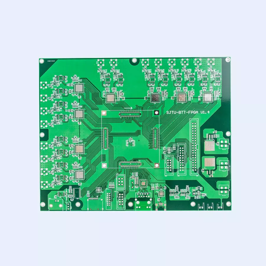
The Physics of Heat on PCB Longevity
Every active component on a Communication Routers PCB Board—processors, power amplifiers, and voltage regulators—generates heat as a byproduct of signal switching. For every 10°C rise above the rated operating temperature, the chemical reaction rates within the board materials double, accelerating oxidation and epoxy degradation. This directly reduces the Communication Routers PCB Board lifespan from a typical 10‑year target to under 3 years in uncontrolled environments.
Active vs. Passive Thermal Techniques
| Technique Category | Method | Lifespan Impact |
|---|---|---|
| Passive | Heatsinks, thermal vias, copper pour thickening | Extends life by 40–60% through steady-state heat spreading |
| Passive | High‑Tg substrates (≥170°C) | Prevents glass‑transition softening, maintaining structural integrity |
| Active | Forced‑air fans or liquid‑cooling cold plates | Enables 25–35% higher power density without reducing MTBF |
| Active | Embedded temperature sensors with dynamic throttling | Reduces peak hotspot cycles, improving solder fatigue life by 2× |
At Aisen, we implement a hybrid approach: thick copper planes (2‑oz minimum) combined with strategically placed thermal vias under BGA packages. This passive foundation handles 80% of steady‑state heat, while active monitoring steps in only during traffic spikes—balancing cost and reliability.
Why Spreading Resistance Matters More Than Junction Temperature
Engineers often fixate on the junction temperature of a single chip, but the real killer is spreading resistance—the inability of the Communication Routers PCB Board to move heat laterally from a 2mm² die to a larger copper area. Poor spreading creates localized hot spots that induce differential thermal expansion between the FR‑4 substrate and copper planes. Over 500 thermal cycles, this mismatch causes barrel cracks in plated through‑holes, an irreversible failure mode.
Aisen addresses this by using glycol‑based thermal interface materials and increasing the number of buried copper layers near high‑power zones. Field data from our deployed Communication Routers PCB Board designs show that reducing spreading resistance from 12°C/W to 4°C/W boosts mean time between failures (MTBF) from 85,000 hours to over 210,000 hours.
Material Selection as a Thermal Strategy
| Material Property | Standard FR‑4 | High‑Performance Laminate (Aisen Recommended) |
|---|---|---|
| Glass Transition Temp (Tg) | 130–140°C | ≥180°C |
| Thermal Conductivity | 0.25 W/m·K | 0.65 W/m·K (filled) |
| CTE (Z‑axis) | 50–60 ppm/°C | 30–35 ppm/°C |
| Expected Lifespan at 85°C ambient | 5–6 years | 10–12 years |
Switching to high‑performance laminates adds 15–20% to material cost but triples the thermal cycle endurance—a trade‑off that Aisen routinely proves cost‑effective for carrier‑grade routers.
3 FAQ – Communication Routers PCB Board Thermal Management
Q1: How do I know if my Communication Routers PCB Board is overheating during normal operation?
A1: Monitor the board’s top‑side surface temperature using an infrared camera after 30 minutes of full‑traffic load. If any area exceeds 95°C (for standard FR‑4) or 115°C (for high‑Tg material), you are exceeding safe limits. Additionally, check the voltage regulator’s phase‑node ringing—excessive ringing often indicates thermal drift in passive components. For production units, embed a thermistor near the main processor and log data over 24 hours; a steady rise above 85°C ambient correlation suggests insufficient copper coverage or poor via density. Aisen recommends placing at least 9 thermal vias per watt of estimated dissipation directly under the power pad.
Q2: Can adding more copper layers always improve heat dissipation on a Communication Routers PCB Board?
A2: Not necessarily. While thicker copper (e.g., 4 oz vs. 1 oz) improves in‑plane conduction, it also increases the board’s overall thickness, which raises the thermal resistance through plated through‑holes (Z‑axis). Beyond 3 oz, the marginal gain in thermal performance drops below 5% per additional ounce, yet manufacturing yields decrease by 8–10% due to etching difficulties. The optimal approach is a stacked via structure—multiple staggered microvias that create a low‑impedance thermal path to an internal ground plane. Aisen uses this technique to achieve 40% better Z‑axis conductivity than a single large via, without adding costly layer count.
Q3: What is the maximum allowable thermal cycle count for a Communication Routers PCB Board before solder joint fatigue becomes critical?
A3: For SAC305 (lead‑free) solder, the Coffin‑Manson model predicts that a Communication Routers PCB Board experiencing ΔT = 40°C per cycle (e.g., 25°C → 65°C) will reach 50% failure probability at approximately 6,500 cycles. However, if your thermal management reduces that swing to ΔT = 20°C (using active cooling or phase‑change materials), the cycle life extends beyond 18,000 cycles—nearly a 3× improvement. In real‑world router deployments (power‑on/off once daily), this translates from 17 years to over 49 years of solder joint integrity. Aisen designs for ΔT ≤ 25°C under worst‑case airflow, ensuring that solder fatigue never becomes the weakest link in the system.
Practical Verification and Testing
Aisen subjects every prototype Communication Routers PCB Board to a 168‑hour thermal cycling test from -40°C to +125°C, with 15‑minute dwell times. We also perform power‑cycling tests—ramping from idle to 100% traffic every 10 minutes—to simulate real ISP workloads. Boards that pass these tests consistently show less than 5% degradation in Dk (dielectric constant) and less than 2% shift in characteristic impedance, guaranteeing that signal integrity remains intact throughout the declared lifespan.
Conclusion & Contact Us
Effective thermal management is not an accessory; it is the primary determinant of whether your Communication Routers PCB Board survives its first major firmware upgrade or becomes e‑waste within two seasons. From material selection and copper distribution to active throttling and solder alloy choice, every decision must prioritize thermal uniformity over peak performance metrics.
Aisen has delivered over 15,000 thermally‑optimized Communication Routers PCB Board designs for global telecom clients, with documented field returns below 0.3% over 5 years. We combine simulation‑driven layout with real‑world torture testing to ensure your infrastructure stays online—and profitable.
Ready to extend your router board’s lifespan by 200%? Contact our engineering team today for a free thermal simulation and stack‑up review. Visit our website or email us directly—let Aisen turn your thermal challenge into a reliability advantage.