

How Do Testing Instruments PCB Improve the Accuracy and Reliability of Electronic Testing?
2026-08-28
Article Summary: Testing instruments PCB are specialized printed circuit boards designed to support measurement, signal processing, control, communication, and data acquisition functions inside electronic testing equipment. Their performance directly affects measurement stability, repeatability, signal integrity, and the overall reliability of a testing system. For manufacturers of oscilloscopes, automated test equipment, laboratory instruments, industrial testers, and other electronic measurement devices, selecting the right PCB design and manufacturing solution is essential. This article explains how Testing Instruments PCB work, what design factors matter most, how manufacturing quality influences test accuracy, and how to choose a reliable PCB manufacturing partner for demanding testing applications.
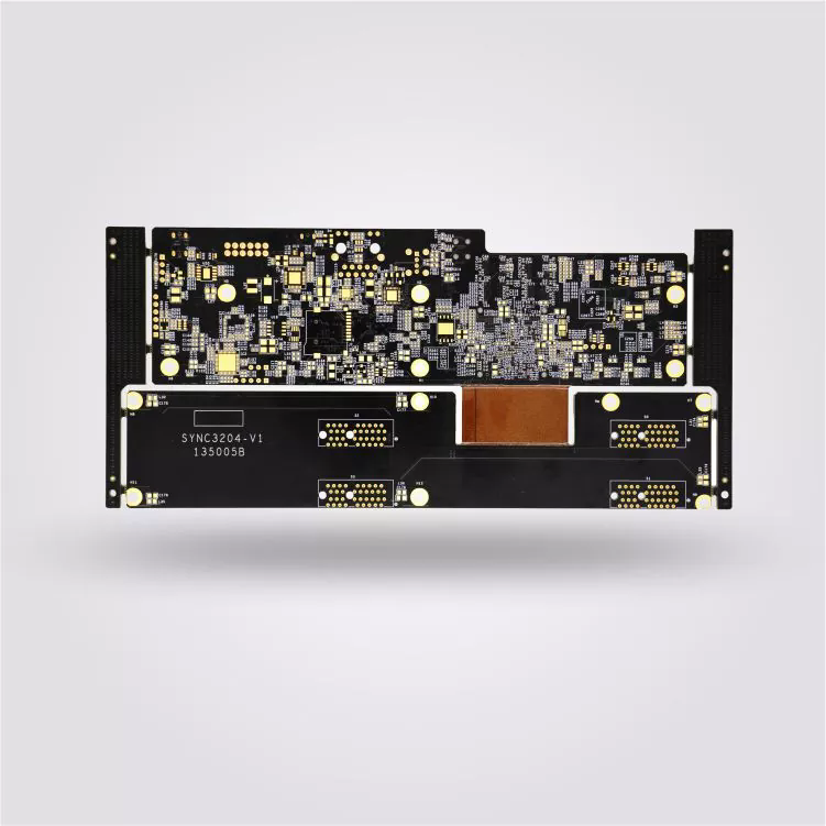
Table of Contents
- 1. What Are Testing Instruments PCB?
- 2. Why Do Testing Instruments Require Specialized PCB Design?
- 3. Where Are Testing Instruments PCB Commonly Used?
- 4. How Should Testing Instruments PCB Be Designed?
- 5. Which PCB Materials Are Suitable for Testing Instruments?
- 6. How Does Signal Integrity Affect Testing Instruments PCB?
- 7. How Does PCB Manufacturing Quality Affect Test Accuracy?
- 8. What Testing Methods Should Be Applied to Testing Instruments PCB?
- 9. What Common Problems Can Testing Instruments PCB Prevent?
- 10. How Can You Choose a Reliable Testing Instruments PCB Manufacturer?
- 11. Key Selection Factors at a Glance
- 12. Conclusion
- 13. FAQ
Article Outline
- Understand the structure and purpose of Testing Instruments PCB.
- Identify the electrical and mechanical requirements of measurement equipment.
- Evaluate materials, stack-up, impedance, grounding, and signal integrity.
- Understand how manufacturing tolerances influence measurement performance.
- Review essential inspection and reliability testing procedures.
- Use practical criteria when selecting a PCB manufacturing partner.
What Are Testing Instruments PCB?
Testing Instruments PCB refers to printed circuit boards engineered specifically for electronic testing and measurement equipment. Unlike ordinary control boards, these PCBs often have to process sensitive analog signals, high-speed digital signals, power circuits, sensor inputs, communication interfaces, and data acquisition functions within the same equipment.
A testing instrument may appear to be a complete enclosure with a display, buttons, connectors, and probes, but the PCB inside is responsible for much of the instrument's actual performance. It provides electrical interconnection between components, establishes signal paths, controls measurement functions, and often performs amplification, filtering, conversion, processing, and communication.
Typical equipment that can use Testing Instruments PCB includes oscilloscopes, multimeters, spectrum analyzers, electronic load testers, laboratory measurement systems, automated test equipment, power analyzers, sensor testing equipment, industrial diagnostic instruments, and specialized production-line inspection equipment.
For these applications, PCB performance is not simply about whether the circuit powers on. The board must help the complete instrument achieve stable measurements and repeatable results over its intended operating conditions.
Why Do Testing Instruments Require Specialized PCB Design?
Testing equipment is fundamentally different from many ordinary electronic products because its purpose is to measure another system accurately. If the PCB introduces excessive noise, unwanted electromagnetic interference, voltage instability, thermal drift, or signal distortion, the instrument may produce incorrect measurements even when the software and external components are functioning correctly.
This makes PCB engineering an important part of measurement-system development.
| Requirement | Why It Matters | Potential Risk if Ignored |
|---|---|---|
| Low electrical noise | Protects weak measurement signals | Unstable or inaccurate readings |
| Controlled impedance | Maintains high-speed signal quality | Reflections and waveform distortion |
| Effective grounding | Reduces unwanted interference | Noise coupling and measurement errors |
| Thermal stability | Reduces temperature-related drift | Measurement variation |
| Reliable assembly | Maintains consistent electrical connections | Intermittent failures and field returns |
A specialized PCB therefore needs to balance electrical performance, manufacturability, component density, thermal management, mechanical constraints, and long-term reliability.
Where Are Testing Instruments PCB Commonly Used?
The application range of Testing Instruments PCB is broad because almost every modern measurement instrument relies on electronic signal processing.
- Oscilloscopes: High-speed signal acquisition and waveform processing require carefully controlled PCB layouts.
- Digital multimeters: Precision measurement circuits require low-noise layouts and stable reference circuits.
- Spectrum analyzers: High-frequency signal paths demand controlled impedance and careful electromagnetic design.
- Power analyzers: Accurate voltage and current acquisition requires suitable isolation, filtering, and thermal considerations.
- Automated test equipment: High channel counts and fast switching require reliable routing and consistent electrical performance.
- Sensor testing equipment: Weak analog signals require protection from interference generated by digital and power circuits.
- Industrial diagnostic instruments: Robust PCB construction helps equipment withstand vibration, temperature changes, and continuous operation.
- Laboratory instruments: Precision components and stable PCB architecture support repeatable measurements.
The exact PCB architecture depends on the instrument's measurement range, bandwidth, resolution, environmental conditions, interface requirements, and applicable safety requirements.
How Should Testing Instruments PCB Be Designed?
A successful Testing Instruments PCB begins with system-level planning rather than simply placing components onto a board. Engineers need to understand how signals enter the instrument, how they are conditioned, where they are converted, how they are processed, and how measurement data is ultimately delivered to the user or another system.
Separate Sensitive and Noisy Circuits
One of the most important principles is separating sensitive analog circuitry from high-speed digital and switching power circuits wherever practical. Digital processors, clocks, switching regulators, and high-current paths can generate noise that interferes with low-level measurement channels.
Good floorplanning can reduce unwanted coupling before additional filtering or shielding becomes necessary.
Build an Appropriate Grounding Strategy
Grounding is particularly important in measurement equipment. An uncontrolled return-current path can create voltage differences between circuit sections and introduce unwanted noise into sensitive signals.
Depending on the instrument architecture, engineers may use carefully planned analog and digital ground regions, solid reference planes, controlled return paths, shielding structures, or isolation techniques. The correct strategy depends on the complete electrical system rather than applying a single universal grounding rule.
Control High-Speed Signal Paths
When a testing instrument contains high-speed interfaces or high-frequency measurement channels, PCB traces become part of the electrical transmission system. Trace width, dielectric thickness, copper geometry, layer structure, vias, connectors, and termination all influence signal behavior.
Controlled-impedance routing can therefore be essential for applications involving fast edges, RF signals, high-speed data interfaces, or precision waveform acquisition.
Consider Thermal Distribution
Temperature affects electronic components and measurement circuits. Components such as voltage references, amplifiers, converters, regulators, and processors may have temperature-dependent characteristics.
A good PCB design considers component placement, copper distribution, thermal vias, heat dissipation paths, and the location of temperature-sensitive circuits. The goal is not merely to keep the board cool but to maintain predictable thermal behavior across the measurement system.
Which PCB Materials Are Suitable for Testing Instruments?
Material selection should be based on electrical, thermal, mechanical, frequency, and environmental requirements.
| Material Consideration | Typical Benefit | Important Application Factor |
|---|---|---|
| Standard FR-4 | Balanced cost and performance | Suitable for many general electronic instruments |
| High-Tg materials | Improved thermal stability | Useful for higher operating temperatures |
| Low-loss materials | Better high-frequency signal behavior | Important for RF and high-speed applications |
| Metal-core structures | Enhanced heat dissipation | Useful where thermal management is critical |
Material selection should be finalized together with the PCB stack-up, component specifications, operating temperature range, signal frequency, and expected service life.
How Does Signal Integrity Affect Testing Instruments PCB?
Signal integrity directly influences the quality of measurement data. A testing instrument may need to detect very small voltage changes while simultaneously operating processors, displays, communication interfaces, and power converters. Without careful signal management, interference can travel through conductive and radiated paths.
Important signal-integrity considerations include:
- Trace impedance and width.
- Reference-plane continuity.
- Return-current paths.
- Via transitions.
- Connector selection.
- Trace length matching where required.
- Analog filtering.
- Power-supply decoupling.
- Electromagnetic compatibility.
- Separation of sensitive and high-noise circuits.
For precision instruments, PCB design should be evaluated as part of the entire signal chain. The objective is not simply to create electrically connected traces but to preserve the intended characteristics of the measured signal from input connector to acquisition circuit.
How Does PCB Manufacturing Quality Affect Test Accuracy?
Even a well-designed PCB can experience performance problems if manufacturing processes are inconsistent. Dimensional variation, poor solder joints, plating defects, contamination, insufficient copper thickness, via problems, or assembly errors can affect electrical performance and long-term reliability.
For Testing Instruments PCB, manufacturing quality can influence:
- Electrical continuity.
- Insulation performance.
- Impedance consistency.
- Connector reliability.
- Component placement accuracy.
- Solder joint integrity.
- Thermal performance.
- Long-term resistance to environmental stress.
This is why PCB production should include controlled processes, documented specifications, appropriate inspection equipment, and traceable quality procedures.
Why Dimensional Control Matters
Precision testing equipment frequently uses dense component placement and fine-pitch packages. Small dimensional deviations can influence assembly quality, connector alignment, or the performance of high-density interconnections.
Why Surface Finish Matters
The PCB surface finish affects solderability, contact reliability, and corrosion resistance. The appropriate finish should be selected according to component packages, assembly process, expected service conditions, and product requirements.
Why Via Reliability Matters
Multilayer Testing Instruments PCB often depend heavily on vias for power distribution, signal transitions, and grounding. Poorly manufactured vias can create intermittent electrical problems that are difficult to diagnose after final equipment assembly.
What Testing Methods Should Be Applied to Testing Instruments PCB?
A reliable testing program should cover both bare-board manufacturing quality and assembled-board functionality. The exact test sequence depends on the design, but several methods are commonly valuable.
| Test Method | Primary Purpose |
|---|---|
| Automated Optical Inspection | Detects visible assembly and component-placement defects |
| Flying Probe Test | Checks electrical connectivity and selected circuit nodes |
| In-Circuit Test | Evaluates components and circuit functions using dedicated test access |
| Functional Test | Confirms the assembled PCB operates according to design requirements |
| Insulation Test | Evaluates electrical isolation where applicable |
| Thermal Evaluation | Identifies abnormal heat generation and thermal concentration |
| Signal Verification | Confirms critical signal paths meet required electrical characteristics |
Combining multiple inspection stages is generally more effective than relying on a single test. Visual inspection may find assembly defects, while electrical and functional testing can identify faults that are invisible to the human eye.
What Common Problems Can Testing Instruments PCB Prevent?
Well-engineered Testing Instruments PCB can address many of the problems that reduce measurement reliability and increase maintenance costs.
- Measurement drift: Appropriate thermal and power design can reduce unwanted variation.
- Signal interference: Better grounding, routing, filtering, and shielding can limit noise coupling.
- Intermittent faults: Reliable soldering, vias, connectors, and inspection processes reduce hidden connection problems.
- Communication errors: Proper high-speed routing helps maintain stable digital interfaces.
- Unexpected heating: Correct component placement and thermal design help manage heat.
- Premature component failure: Appropriate electrical and thermal margins improve service reliability.
- Production inconsistency: Controlled manufacturing processes improve board-to-board repeatability.
These improvements are particularly valuable for instruments used in laboratories, factories, quality-control departments, and automated production environments where measurement repeatability directly affects production decisions.
How Can You Choose a Reliable Testing Instruments PCB Manufacturer?
Selecting a PCB supplier should involve more than comparing unit prices. Testing equipment often requires close cooperation between the customer's electrical engineers, PCB layout engineers, component engineers, and manufacturing team.
When evaluating a supplier such as Shenzhen Aisen Electronics Co.,Ltd., customers should consider the manufacturer's ability to understand the technical requirements of the complete product rather than treating the PCB as an isolated commodity.
Key evaluation points include:
- Engineering capability: The supplier should understand multilayer design, signal integrity, power distribution, thermal management, and manufacturability.
- Production capability: Equipment and processes should match the board's layer count, line width, spacing, hole structure, material, and surface-finish requirements.
- Quality control: Inspection procedures should be defined according to the risks associated with the product.
- Communication: Engineering questions should be addressed clearly before production begins.
- Traceability: Production information and inspection records can make troubleshooting and quality management more efficient.
- Customization: Testing instruments often require application-specific board structures, so flexible manufacturing support is valuable.
- Delivery consistency: Stable production planning is important when PCB assemblies are part of a larger equipment manufacturing schedule.
A supplier that can participate early in the design-for-manufacturing process may also help identify potential production problems before they become expensive engineering changes.
Key Selection Factors at a Glance
| Factor | What to Evaluate | Why It Matters |
|---|---|---|
| PCB Structure | Layers, thickness, vias, spacing | Determines electrical and mechanical compatibility |
| Material | FR-4, high-Tg, low-loss or specialized materials | Influences thermal and electrical performance |
| Signal Integrity | Impedance, routing, return paths | Protects measurement accuracy |
| Assembly | Component placement and solder quality | Improves reliability and repeatability |
| Inspection | AOI, electrical testing, functional testing | Reduces defects reaching final assembly |
| Customization | Ability to accommodate application-specific requirements | Supports specialized test equipment |
Conclusion
Testing Instruments PCB is a critical foundation for modern measurement and diagnostic equipment. Because testing instruments are expected to produce reliable and repeatable data, their internal PCBs must provide more than basic electrical connectivity. Signal integrity, grounding, thermal management, material selection, manufacturing precision, component assembly, and inspection all contribute to the final performance of the instrument.
The most effective approach is to treat PCB development as part of the complete measurement system. Engineers should define electrical requirements early, establish appropriate PCB architecture, select suitable materials, control sensitive signal paths, and implement verification procedures that reflect the actual operating conditions of the equipment.
For manufacturers developing new testing equipment or improving an existing product, working with an experienced PCB partner can simplify the transition from design to stable mass production. Shenzhen Aisen Electronics Co.,Ltd. can be considered when you need a PCB manufacturing solution tailored to the technical requirements of testing and measurement applications.
Looking for a dependable Testing Instruments PCB solution for your next project? Discuss your PCB specifications, application requirements, production volume, and quality expectations with Shenzhen Aisen Electronics Co.,Ltd. to identify a suitable manufacturing approach and contact us for professional support.
FAQ
What is a Testing Instruments PCB?
A Testing Instruments PCB is a printed circuit board designed for electronic measurement and testing equipment. It can support signal acquisition, amplification, filtering, conversion, processing, control, power distribution, and communication functions.
Why is PCB design important for measurement accuracy?
PCB layout influences noise, interference, impedance, grounding, thermal behavior, and signal transmission. Poor PCB design can introduce errors into the measurement chain, while a carefully engineered board helps maintain stable and repeatable signals.
Can Testing Instruments PCB support high-frequency applications?
Yes. With suitable materials, controlled-impedance routing, appropriate stack-up design, carefully managed return paths, and appropriate components and connectors, PCBs can be engineered for high-frequency and high-speed testing applications.
What PCB material should be used for testing equipment?
There is no single material suitable for every instrument. Standard FR-4 can meet many general requirements, while high-Tg or low-loss materials may be appropriate for applications involving higher temperatures or demanding high-frequency performance. Material selection should follow the electrical and environmental requirements of the specific instrument.
How can PCB noise be reduced in testing equipment?
Common approaches include separating sensitive analog and noisy digital circuits, improving grounding and return-current paths, using suitable power decoupling, controlling high-speed routing, adding appropriate filtering, and considering shielding or isolation where necessary.
What tests should be performed on Testing Instruments PCB?
Depending on the product, inspection may include automated optical inspection, electrical continuity testing, flying-probe testing, in-circuit testing, functional testing, insulation testing, thermal evaluation, and signal verification.
Why should I work with an experienced PCB manufacturer?
Testing equipment often combines precision analog circuits, high-speed digital interfaces, power systems, and mechanical constraints. An experienced PCB manufacturer can help evaluate manufacturability, production tolerances, material requirements, assembly risks, and inspection strategies before these issues affect production.
Can Testing Instruments PCB be customized?
Yes. Testing equipment frequently requires customized board dimensions, layer structures, component configurations, connector locations, impedance requirements, thermal solutions, and assembly processes. The final PCB should be developed around the requirements of the complete instrument.
What should I provide when requesting a Testing Instruments PCB quotation?
Useful information includes PCB drawings or Gerber files, BOM data, board dimensions, layer count, material requirements, surface finish, quantity, assembly requirements, testing specifications, electrical requirements, and any special reliability or environmental conditions.
How can Shenzhen Aisen Electronics Co.,Ltd. support a Testing Instruments PCB project?
Shenzhen Aisen Electronics Co.,Ltd. can be approached for PCB manufacturing and customized production requirements related to testing and measurement applications. Providing complete technical documentation at the beginning of a project allows the manufacturing team to evaluate the board requirements more effectively and develop an appropriate production plan.
How Will Testing Instruments PCB Develop in Future Electronic Industries?
The demand for higher measurement accuracy, faster data processing, smaller equipment sizes, and more intelligent testing solutions continues to increase across many industries. As electronic products become more complex, Testing Instruments PCB must also evolve to support advanced measurement technologies and stricter performance expectations.
Future testing equipment will require PCB solutions that combine higher integration levels, improved signal management, stronger reliability, and better manufacturing flexibility. These trends are especially important in industries such as semiconductor manufacturing, automotive electronics, aerospace systems, medical devices, renewable energy equipment, and industrial automation.
Several important development directions are influencing the next generation of Testing Instruments PCB:
- Higher-density PCB structures: More functions are being integrated into smaller instruments, requiring advanced multilayer PCB technologies, microvias, and high-density interconnection solutions.
- Faster signal processing capability: Modern testing systems require higher bandwidth and faster communication interfaces, increasing the importance of controlled impedance and signal integrity design.
- Improved electromagnetic compatibility: As electronic environments become more crowded, PCB designs need stronger protection against electromagnetic interference.
- Intelligent monitoring functions: Testing instruments increasingly include embedded processors, wireless communication, cloud connectivity, and automated analysis capabilities.
- Higher reliability requirements: Industrial and laboratory equipment often operates continuously, making long service life and stable performance essential.
Manufacturers that understand these trends can better prepare their PCB platforms for future product generations. Cooperation between equipment developers and PCB specialists during early design stages can help reduce development risks and improve final product performance.
How Can Testing Instruments PCB Help Reduce Overall Equipment Costs?
Although high-quality PCB manufacturing may require careful engineering investment, a reliable Testing Instruments PCB can help reduce total equipment costs throughout the product lifecycle.
Many companies focus only on the initial PCB price, but the actual cost of a testing system also includes development time, production efficiency, maintenance expenses, warranty claims, and equipment downtime.
| Cost Area | PCB Contribution | Long-Term Benefit |
|---|---|---|
| Product Development | Professional PCB engineering reduces design problems | Shorter development cycles |
| Manufacturing | Optimized PCB design improves assembly efficiency | Lower production waste |
| Maintenance | Reliable PCB structures reduce failures | Lower service costs |
| Equipment Operation | Stable electrical performance improves uptime | Higher customer satisfaction |
A properly engineered PCB can prevent many expensive problems before the equipment reaches customers. This is especially important for professional testing systems where downtime can affect laboratory research, factory production, or quality inspection processes.
What Quality Factors Should Be Checked Before Mass Production?
Before moving from prototype development to volume manufacturing, companies should perform a detailed review of the Testing Instruments PCB design and production plan.
Important quality checkpoints include:
- Design verification: Confirm that schematic design, PCB layout, component selection, and electrical requirements are consistent.
- Manufacturing review: Check whether board thickness, layer structure, drilling requirements, and assembly processes are suitable for production.
- Component compatibility: Ensure that selected components match assembly capabilities and long-term supply requirements.
- Prototype validation: Evaluate actual PCB performance before large-scale manufacturing.
- Reliability testing: Confirm operation under expected temperature, workload, and environmental conditions.
- Production consistency: Establish inspection standards to maintain stable quality between different production batches.
A detailed validation process can significantly reduce the possibility of redesign, production delays, and unexpected field failures.
How Does Engineering Support Improve Testing Instruments PCB Projects?
Testing equipment development usually involves multiple engineering disciplines, including circuit design, mechanical engineering, software development, firmware programming, and manufacturing engineering. PCB suppliers that provide strong technical communication can help connect these different areas.
During a PCB project, engineering support may include:
- Reviewing PCB files and identifying manufacturing risks.
- Suggesting suitable materials and stack-up structures.
- Evaluating signal integrity requirements.
- Improving component placement and routing efficiency.
- Supporting prototype production and testing adjustments.
- Optimizing the design for future mass production.
For specialized applications, this engineering cooperation can be a major factor in achieving stable product performance. Shenzhen Aisen Electronics Co.,Ltd. focuses on providing customized PCB manufacturing support for customers with different electronic application requirements, helping businesses transform technical concepts into reliable PCB products.
How Can Proper PCB Design Improve Testing Equipment Maintenance?
Maintenance efficiency is an important consideration for professional testing equipment. Instruments used in industrial environments, research facilities, and production lines may operate for thousands of hours, making serviceability an important product feature.
Good Testing Instruments PCB design can support easier maintenance through:
- Clear circuit organization.
- Reliable connector selection.
- Accessible test points.
- Stable power distribution.
- Protection against electrical stress.
- Improved fault diagnosis capability.
When engineers can quickly identify and repair potential issues, equipment downtime can be reduced. This improves operational efficiency and extends the useful service life of testing systems.
Final Summary: Why Testing Instruments PCB Matters
Testing Instruments PCB plays a fundamental role in determining the accuracy, stability, and reliability of electronic measurement equipment. From signal acquisition and processing to power management and communication, every PCB design decision can influence the final performance of a testing system.
Successful Testing Instruments PCB development requires careful consideration of electrical design, material selection, manufacturing capability, inspection methods, and long-term reliability. Companies that invest in high-quality PCB solutions can achieve more dependable instruments, reduce maintenance challenges, and improve customer confidence.
With growing demand for precision measurement and intelligent testing technologies, choosing an experienced PCB partner becomes increasingly important. Shenzhen Aisen Electronics Co.,Ltd. provides customized PCB solutions designed to meet the requirements of modern testing equipment applications. If you are developing new measurement products or looking for a reliable PCB manufacturing solution, please contact us to discuss your project requirements and receive professional support.